SPRUIS4E March 2022 – January 2024
- 1
- Jacinto7 J721E/DRA829/TDA4VM Evaluation Module (EVM)
- Trademarks
- 1Introduction
- 2J721E EVM Overview
- 3EVM User Setup/Configuration
-
4J721E EVM Hardware Architecture
- 4.1 J721E EVM Hardware Top level Diagram
- 4.2 J721E EVM Interface Mapping
- 4.3 I2C Address Mapping
- 4.4 GPIO Mapping
- 4.5 Power Supply
- 4.6 Reset
- 4.7 Clock
- 4.8 Memory Interfaces
- 4.9 MCU Ethernet Interface
- 4.10 QSGMII Ethernet Interface
- 4.11 PCIe Interface
- 4.12 USB Interface
- 4.13 CAN Interface
- 4.14 FPD Interface (Audio Deserializer)
- 4.15 FPD Panel Interface (DSI Video Serializer)
- 4.16 Display Serial Interface (DSI) FPC
- 4.17 Audio Interface
- 4.18 Display Port Interface
- 4.19 MLB Interface
- 4.20 I3C Interface
- 4.21 ADC Interface
- 4.22 RTC Interface
- 4.23 Apple Authentication Header
- 4.24 EVM Expansion Connectors
- 4.25 ENET Expansion Connector
- 4.26 CSI Expansion Connector
- 5Revision History
3.2.2 Power Regulators and Power Status LEDs
The processor Card utilizes an array of DC-DC converters to supply the various memories, clocks and other components on the Card with the necessary voltage and the power required.
Dual Buck controller LM5140-Q1 provides the primary stage power conversion (12 V to 5 V / 3.3 V). These 3.3 V and 5 V is the primary voltages for the SoM power management resources.
Buck-Boost controller LM5175 and another Buck controller LM5141 provides 12 V and 3.3 V supplies to the expansion connectors. The power good signals of these power regulators are used to generate the SoC PORz.
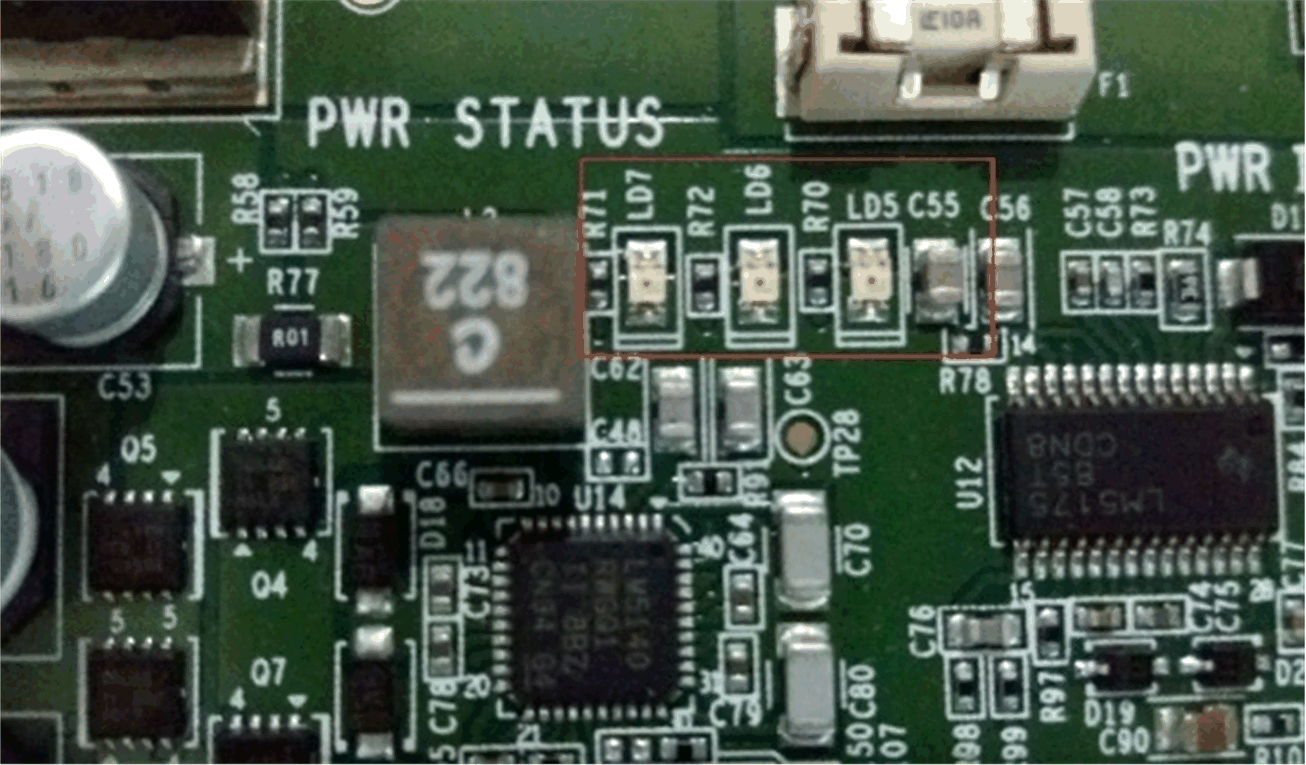
Multiple power-indication LEDs are provided on board to give users positive confirmation of the status of output of major supplies. The LEDs indicated power in the various domains.
| Sl No | LED | Power Status | Sch Net Name |
|---|---|---|---|
| 1 | LD2 | Input Power On/Off | VINPUT |
| 2 | LD7 | Regulated Power On/Off | VSYS_3V3 |
| 3 | LD5 | SoC Main Domain On/Off | VSYS_IO_3V3 |
| 4 | LD6 | SoC MCU Domain On/Off | VSYS_MCUIO_3V3 |
 Figure 3-4 Power Status LEDs
Test points for each system power rails are provided on the Common Processor Board (CPB) and are mentioned in Table 3-4. Location for each can be identified by searching the assembly drawing for the test point reference number.
| Power Supply | Test Point | Nominal Voltage |
|---|---|---|
| VINPUT | TP20 | 12.0V |
| VSYS_3V3 | TP130 | 3.3V |
| VCC_12V0 | TP39 | 12.0V |
| VSYS_5V0 | TP26 | 5.0V |
| EXP_3V3 | TP43 | 3.3V |
| VDD_2V5 | TP63 | 2.5V |
| VDD_1V0 | TP59 | 1.0V |
| VCC_1V1 | TP60 | 1.1V |
| VSYS_MCU_5V0 | TP117 | 5.0V |
| VDD_SD_DV | TP44 | 3.3V |
| VSYS_MCUIO_3V3 | TP113 | 3.3V |
| VSYS_IO_3V3 | TP131 | 3.3V |
| VSYS_MCUIO_1V8 | TP134 | 1.8V |
| VSYS_IO_1V8 | TP132 | 1.8V |
| VDA_MCU_1V8 | TP105 | 1.8V |