SPRUIS4E March 2022 – January 2024
- 1
- Jacinto7 J721E/DRA829/TDA4VM Evaluation Module (EVM)
- Trademarks
- 1Introduction
- 2J721E EVM Overview
- 3EVM User Setup/Configuration
-
4J721E EVM Hardware Architecture
- 4.1 J721E EVM Hardware Top level Diagram
- 4.2 J721E EVM Interface Mapping
- 4.3 I2C Address Mapping
- 4.4 GPIO Mapping
- 4.5 Power Supply
- 4.6 Reset
- 4.7 Clock
- 4.8 Memory Interfaces
- 4.9 MCU Ethernet Interface
- 4.10 QSGMII Ethernet Interface
- 4.11 PCIe Interface
- 4.12 USB Interface
- 4.13 CAN Interface
- 4.14 FPD Interface (Audio Deserializer)
- 4.15 FPD Panel Interface (DSI Video Serializer)
- 4.16 Display Serial Interface (DSI) FPC
- 4.17 Audio Interface
- 4.18 Display Port Interface
- 4.19 MLB Interface
- 4.20 I3C Interface
- 4.21 ADC Interface
- 4.22 RTC Interface
- 4.23 Apple Authentication Header
- 4.24 EVM Expansion Connectors
- 4.25 ENET Expansion Connector
- 4.26 CSI Expansion Connector
- 5Revision History
4.23 Apple Authentication Header
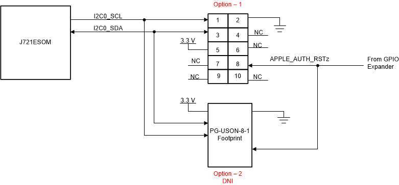
The common processor board has a provision to support Apple authentication interface. In the J721E EVM, the Apple authentication board can be interfaced with J721E SoC in two options: one is module interface and the other is device interface.
 Figure 4-42 Apple Authentication Block Diagram
Module Interface:
Common Processor board have a 2.54 mm Dual row 10 Pin Receptacle Mfr. Part# 2214BR‐10G.
I2C0 Port of J721E SoC and Reset from GPIO Expander is terminated to this connector. 3.3 V supply is provided to the connector J9.
Table 4-27 lists detailed signal and pin descriptions.
| Pin No | Signal | Description |
|---|---|---|
| 1 | I2C0_SCL | I2C slave interface, clock connection |
| 3 | I2C0_SDA | I2C slave interface, data connection |
| 8 | APPLE_AUTH_RSTz | Reset, Active low |
| 5 | VSYS_IO_3V3 | Power 3.3 V |
| 2 | DGND | Ground |
| 4,6,7,9,10 | NC | Not Connected |
Device Interface:
In this approach Common Processor PCB have a footprint PG‐USON‐8‐1. Apple authentication device will not be assembled to this footprint by default.
Required I2C0, Power, Reset and Ground signals from J721E SoC is routed to this footprint, as shown in Table 4-28.
| Pin No | Signal | Description |
|---|---|---|
| 6 | I2C0_SCL | I2C slave interface, clock connection |
| 2 | I2C0_SDA | I2C slave interface, data connection |
| 7 | APPLE_AUTH_RSTz | Reset, Active low |
| 8 | VSYS_IO_3V3 | Power 3.3 V |
| 1, 9 | DGND | Ground |
| 3,4,5 | NC | Not Connected |