SPRUIW7A October   2020  – February 2022


  1.   Trademarks
  2. 1Introduction
    1. 1.1 Key Features
    2. 1.2 Thermal Compliance
    3. 1.3 REACH Compliance
    4. 1.4 Electrostatic Discharge (ESD) Compliance
  3. 2J7200 EVM Overview
    1. 2.1 J7200 EVM Board Identification
    2. 2.2 J7200 SOM Component Identification
    3. 2.3 Jacinto7 Common Processor Component Identification
    4. 2.4 Quad Ethernet Components Identification
  4. 3EVM User Setup/Configuration
    1. 3.1 Power Requirements
    2. 3.2 Power ON Switch and Power LEDs
      1. 3.2.1 Over Voltage and Under Voltage Protection Circuit
      2. 3.2.2 Power Regulators and Power Status LEDs
    3. 3.3 EVM Reset/Interrupt Push Buttons
    4. 3.4 EVM DIP Switches
      1. 3.4.1 EVM Configuration DIP Switch
      2. 3.4.2 SOM Configuration DIP Switch
      3. 3.4.3 Boot Modes
      4. 3.4.4 Other Selection Switches
    5. 3.5 EVM UART/COM Port Mapping
  5. 4J7200 EVM Hardware Architecture
    1. 4.1  J7200 EVM Hardware Top Level Diagram
    2. 4.2  J7200 EVM Interface Mapping
    3. 4.3  I2C Address Mapping
    4. 4.4  GPIO Mapping
    5. 4.5  Power Supply
      1. 4.5.1 Power Sequencing
      2. 4.5.2 Voltage Supervisor
      3. 4.5.3 DDR I/O Voltage Selection
      4. 4.5.4 J7200 SoC SLEEP Logic Operation
      5. 4.5.5 J7200 SoC MCU Only Operation
      6. 4.5.6 J7200 SoC GPIO Retention Operation
      7. 4.5.7 J7200 SoC DDR Retention Operation
      8. 4.5.8 Power Monitoring
      9. 4.5.9 Power Test Points
    6. 4.6  Reset
    7. 4.7  Clock
      1. 4.7.1 Processor’s Primary Clock
      2. 4.7.2 Processor’s Secondary/SERDES Ref Clock
      3. 4.7.3 EVM Peripheral Ref Clock
    8. 4.8  Memory Interfaces
      1. 4.8.1 LPDDR4 Interface
      2. 4.8.2 OSPI Interface
      3. 4.8.3 MMC Interface
        1. 4.8.3.1 MMC0 - eMMC Interface
        2. 4.8.3.2 MMC1 – Micro SD Interface
      4. 4.8.4 Board ID EEPROM Interface
      5. 4.8.5 Boot EEPROM Interface
    9. 4.9  MCU Ethernet Interface
      1. 4.9.1 Gigabit Ethernet PHY Default Configuration
    10. 4.10 QSGMII Ethernet Interface
    11. 4.11 PCIe Interface
      1. 4.11.1 X2 Lane PCIe Interface
    12. 4.12 USB Interface
      1. 4.12.1 USB 3.1 Interface
      2. 4.12.2 USB 2.0 Interface
        1. 4.12.2.1 To PCIe Card Wi-Fi/BT
        2. 4.12.2.2 To Expansion Connector
      3. 4.12.3 USB 3.0 Micro AB Interface (Reserved Port)
    13. 4.13 Audio Interface
      1. 4.13.1 Line IN Port
      2. 4.13.2 MIC Input Port
      3. 4.13.3 Line Out Port
      4. 4.13.4 Head Phone Port
      5. 4.13.5 Port Mapping
    14. 4.14 CAN Interface
      1. 4.14.1 MCU CAN0
      2. 4.14.2 MCU CAN1
      3. 4.14.3 MAIN CAN3 (supports WAKE function)
      4. 4.14.4 MAIN CAN0
    15. 4.15 FPD Interface (Audio Deserializer)
    16. 4.16 I3C Interface
      1. 4.16.1 Gyroscope
      2. 4.16.2 I3C Header
    17. 4.17 ADC Interface
    18. 4.18 RTC Interface
    19. 4.19 Apple Authentication Header
      1. 4.19.1 Module Interface
    20. 4.20 JTAG Emulation
    21. 4.21 EVM Expansion Connectors
    22. 4.22 ENET Expansion Connector
      1. 4.22.1 Power Requirements
      2. 4.22.2 Clock
        1. 4.22.2.1 Main Clock
        2. 4.22.2.2 Optional Clock
      3. 4.22.3 Reset Signals
      4. 4.22.4 Ethernet Interface
        1. 4.22.4.1 Quad Port SGMII PHY Default Configuration
      5. 4.22.5 Board ID EEPROM Interface
  6. 5Functional Safety
  7. 6Revision History

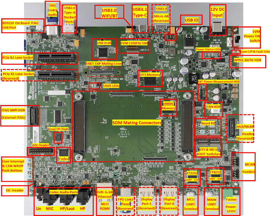
Jacinto7 Common Processor Component Identification
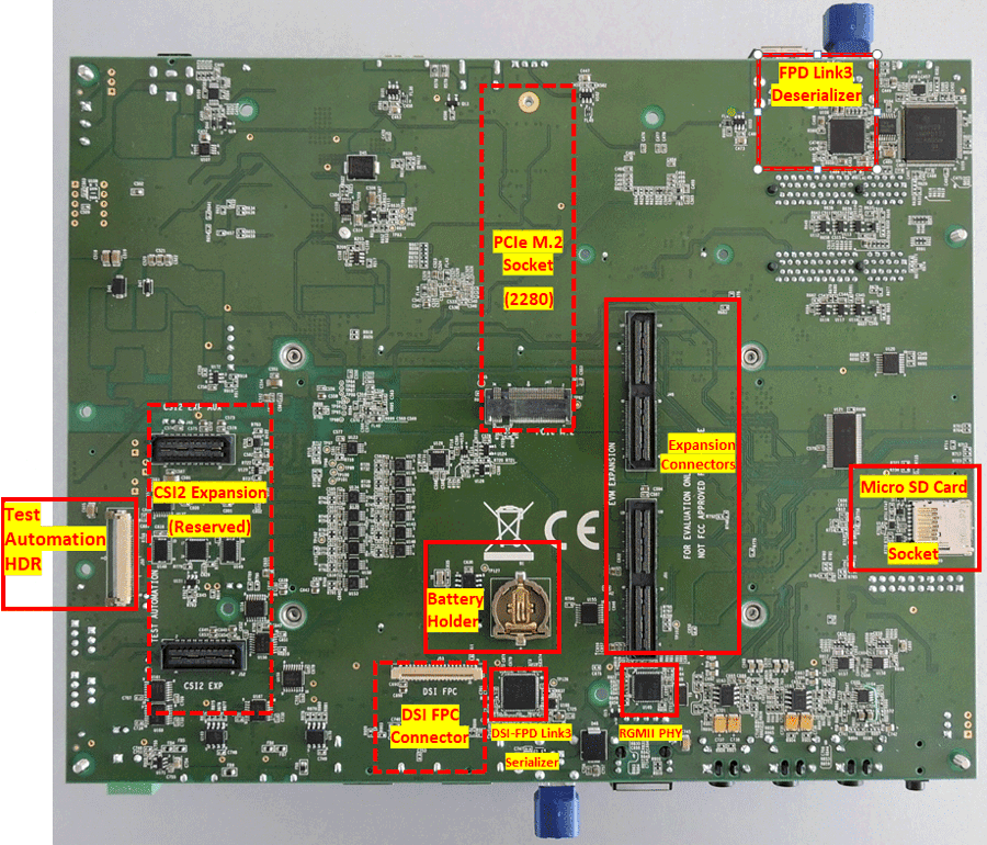
GUID-20200921-CA0I-3L2F-WFXS-N32JBFGF46LW-low.png GUID-20200921-CA0I-JJ3C-3BXN-J6GM4VXJT3ZZ-low.png Figure 2-5 Jacinto7 Common Processor Component Identification

Because the Jacinto7 Common Processor board is used with different SOM boards featuring different Jacinto7 processors with different feature sets, some of the board’s peripherals/interfaces may not be supported. For the J7200 SOM, the following interfaces are not supported:

  • USB 3.0 uAB
  • Display Port 0
  • Display Port 1
  • FPD deserializer
  • PCIe M.2
  • PCIe x1
  • DSI interface
  • UFS
  • MLB
  • CSI2