SPRUIY1D November 2020 – August 2024
- 1
- Description
- Features
- 4
- 1Evaluation Module Overview
-
2Hardware
- 2.1 Board Setup
- 2.2 Hardware Description
- 2.3 Connectors
- 2.4 Mechanical Mounting of the PCB
- 3Additional Information
- 4Revision History
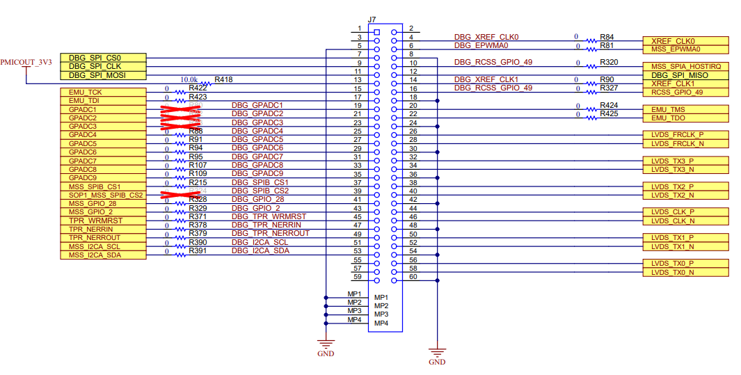
2.3.4 Debug Connector 60-Pin (J7)
This connector enables interfacing of LVDS signals to the DCA1000 EVM for data capturing purposes as well as SPI, I2C, JTAG, GPADC, and other control signals from the AM273x EVM for debug purposes.
The SPI interface must be muxed to the Debug Connector. For more details, refer to Section 2.1.3.

Figure 2-28 Debug Connector Schematic
Table 2-14 J7 Connector Pin
| Pin Number | Description | Pin Number | Description |
|---|---|---|---|
| 1 | NC | 2 | NC |
| 3 | NC | 4 | XREF_CLK0 |
| 5 | GND | 6 | MSS_EPWMA0 |
| 7 | MSS_SPIB_CS0 | 8 | GND |
| 9 | MSS_SPIB_CLK | 10 | MSS_SPIA_HOSTIRQ |
| 11 | MSS_SPIB_PICO | 12 | MSS_SPIB_POCI |
| 13 | 3.3V PULL_UP | 14 | XREF_CLK1 |
| 15 | EMU_TCK | 16 | RCSS_GPIO_49 |
| 17 | EMU_TDI | 18 | GND |
| 19 | GPADC1 | 20 | EMU_TMS |
| 21 | GPADC2 | 22 | EMU_TDS |
| 23 | GPADC3 | 24 | GND |
| 25 | GPADC4 | 26 | LVDS_FRCLK_P |
| 27 | GPADC5 | 28 | LVDS_FRCLK_N |
| 29 | GPADC6 | 30 | GND |
| 31 | GPADC7 | 32 | LVDS_TX3_P |
| 33 | GPADC8 | 34 | LVDS_TX3_N |
| 35 | GPADC9 | 36 | GND |
| 37 | MSS_SPIB_CS1 | 38 | LVDS_TX2_P |
| 39 | SOP1_MSS_SPIB_CS2 | 40 | LVDS_TX2_N |
| 41 | MSS_GPI0_28 | 42 | GND |
| 43 | MSS_GPI0_2 | 44 | LVDS_CLK_P |
| 45 | TPR_WRMRST | 46 | LVDS_CLK_N |
| 47 | TPR_NERRIN | 48 | GND |
| 49 | TPR_NERROUT | 50 | LVDS_TX1_P |
| 51 | MSS_I2CA_SCL | 52 | LVDS_TX1_N |
| 53 | MSS_I2CA_SDA | 54 | |
| 55 | NC | 56 | LVDS_TX0_P |
| 57 | NC | 58 | LVDS_TX0_N |
| 59 | NC | 60 | GND |