-
AM64x and AM243x BGA Escape Routing
AM64x and AM243x BGA Escape Routing
Trademarks
Sitara is a trademark of Texas Instruments Incorporated.
All trademarks are the property of their respective owners.
1 Stackup
The PCB layout designer must balance many different requirements when starting a PCB layout. The first is the board stackup. The AM64x and AM243x devices have a 17.2-mm × 17.2-mm package which has a 0.80-mm pitch ball array of 21×21. To minimize cost, this ball grid is a solid array. Due to the number of rows of signal balls around the periphery, designs must have two routing layers, not counting the top and bottom layers, which can also contain some signal routes. Also, due to the number of power supply rails, there must be two layers dedicated for power planes. Ground planes must be added adjacent to the power planes and adjacent to the outer layers for shielding and controlled impedance routing. High-speed interfaces such as the SERDES and the DDR require ground planes for impedance matching. Due to the higher speeds, ground layers both above and below the DDR signals are recommended. The AM64 GP EVM design connected all of the signal balls and included the additional ground planes. The routing was achieved with 10 layers as shown in Table 1-1.
| PCB Layer | Layer Routing, Planes or Pours |
|---|---|
| Layer 1 | Component pads and signal routing |
| Layer 2 | Ground |
| Layer 3 | Signal routing(1) |
| Layer 4 | Ground |
| Layer 5 | Power |
| Layer 6 | Power |
| Layer 7 | Ground |
| Layer 8 | Signal routing(1) |
| Layer 9 | Ground |
| Layer 10 | Component pads (including most decoupling) and signal routing |
A 10-layer stack-up similar to the one above is needed for relatively dense PCBs. Alternately, the layer count can be reduced, assuming one or more of the following exist:
- The PCB is not crowded around the AM64x or AM243x device. This allows for more routing away from the device on the top and bottom layers, which can reduce layer congestion.
- Many of the signal balls are unused. Many designs do not use all of the interfaces, resulting in unused signal balls. This also reduces routing congestion.
- The PCB layout team has time to carefully place the routes. This can be very time consuming.
It is not acceptable to violate routing rules simply to save money on reduced PCB layers or due to limited routing time. All requirements must still be met. Also, creative routing increases design validation time, both in simulation and bench testing. This can be minimized if the layout is similar to one of the AM64x EVM designs.
The AM64x EVM is implemented in a 10-layer stack-up, similar to the one described in Table 1-1. This design has nearly every signal ball routed to circuitry or a connector. This drives the requirement for the full number of layers. Additionally, this board is designed for optimum signal integrity on the high-speed interfaces while limiting the board size. The AM64x EVM is implemented without a High Density Interconnect (HDI) and does not use microvias. All vias on the AM64x EVM pass completely through the board. This complicates the escape from the BGA.
2 Floorplan Component Placement
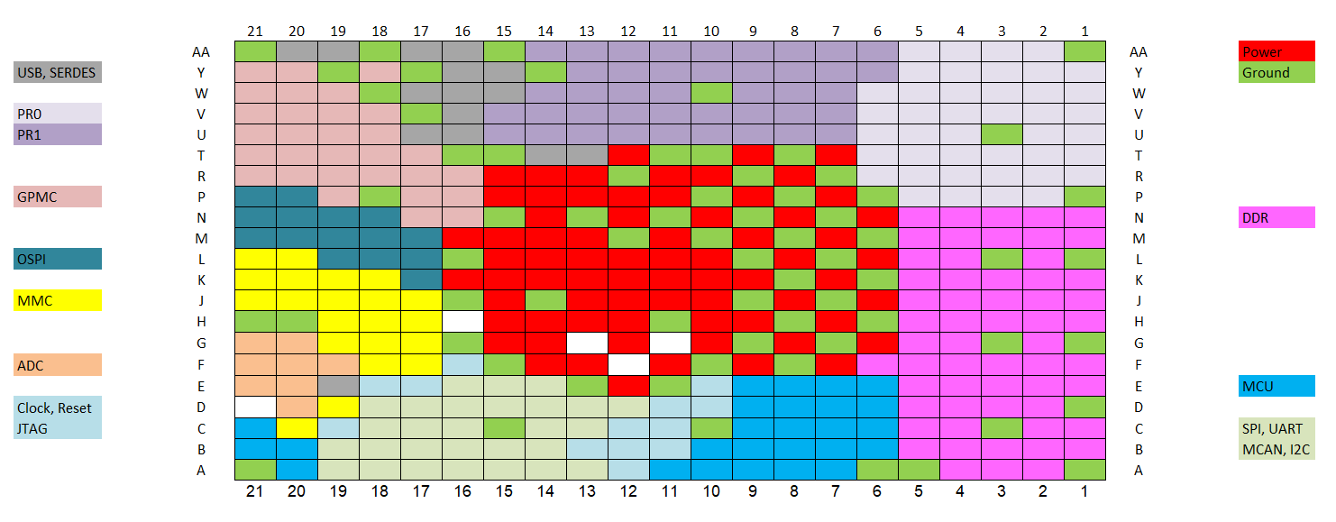
Optimum trace routing will have routes as short as possible with a minimum of cross-over. This requires careful placement of the components around the SoC. Figure 2-1 shows the default arrangement of the signal balls and the power and ground balls. Some of the interfaces can move to other locations due to pin multiplex choices, and there are other interfaces not listed that are exposed through pin multiplex choices. The PCB layout team must analyze the locations of the interfaces used and the associated components or connectors.
 Figure 2-1 AM64x Floorplan