SPRUIY5A February 2021 – July 2021 AM2431 , AM2432 , AM2434 , AM6411 , AM6412 , AM6421 , AM6422 , AM6441 , AM6442
2 Floorplan Component Placement
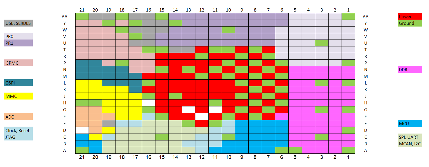
Optimum trace routing will have routes as short as possible with a minimum of cross-over. This requires careful placement of the components around the SoC. Figure 2-1 shows the default arrangement of the signal balls and the power and ground balls. Some of the interfaces can move to other locations due to pin multiplex choices, and there are other interfaces not listed that are exposed through pin multiplex choices. The PCB layout team must analyze the locations of the interfaces used and the associated components or connectors.
 Figure 2-1 AM64x Floorplan