SPRUIY9B May 2021 – October 2023
- 1
- Abstract
- Trademarks
- 1Key Features
- 2EVM Revisions and Assembly Variants
- 3Important Usage Notes
-
4System Description
- 4.1 Key Features
- 4.2 Functional Block Diagram
- 4.3 Power-On/Off Procedures
- 4.4
Peripheral and Major Component
Description
- 4.4.1 Clocking
- 4.4.2 Reset
- 4.4.3 Power
- 4.4.4 Configuration
- 4.4.5 JTAG
- 4.4.6 Test Automation
- 4.4.7 UART Interface
- 4.4.8 Memory Interfaces
- 4.4.9 Ethernet Interface
- 4.4.10 USB 3.0 Interface
- 4.4.11 PRU Connector
- 4.4.12 User Expansion Connector
- 4.4.13 MCU Connector
- 4.4.14 Interrupt
- 4.4.15 I2C Interface
- 4.4.16 IO Expander (GPIOs)
-
5Known Issues
- 5.1 Issue 1: LP8733x Max output Capacitance Spec Exceeded on LDO0 and LDO1
- 5.2 Issue 2: LP8733x Output Voltage of 0.9V Exceeds AM64x VDDR_CORE max Voltage Spec of 0.895 V
- 5.3 Issue 3 - SDIO Devices on MMC0 Require Careful Trace Lengths to Meet Interface Timing Requirements
- 5.4 Issue 4 - LPDDR4 Data Rate Limitation in Stressful Conditions
- 5.5 Issue 5 - Junk Character
- 5.6 Issue 6 - Test Power Down Signal Floating
- 5.7 Issue 7 - uSD Boot Not Working
- 6Regulatory Compliance
- 7Revision History
4.4.9.1 DP83867 PHY Default Configuration
The DP83867 PHY uses four level configurations based on resistor strapping which generate four distinct voltages ranges. The resistors are connected to the RX data and control pins which are normally driven by the PHY and are inputs to the AM64x. The voltage range for each mode is shown below.
Mode 1 - 0 V to 0.3234V
Mode 2 – 0.462V to 0.6303V
Mode 3 – 0.7425V to 0.9372V
Mode 4 – 2.2902V to 2.904V
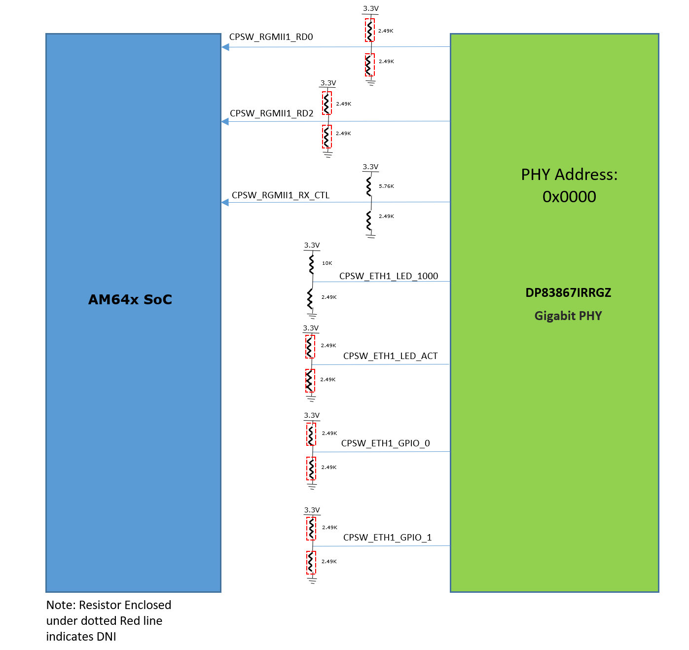
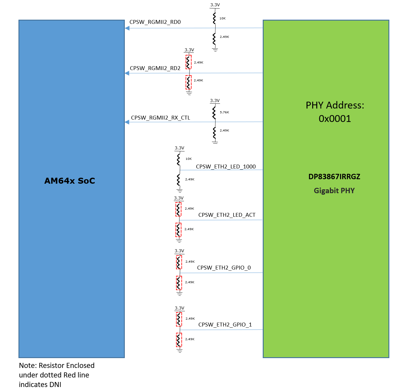
DP83867 device includes internal pull-down resistor. The value of the external pull resistors is selected to provide voltage at the pins of the AM64x as close to ground or 3.3V as possible. The strapping is shown in Figure 4-19. The strap values are given in Table 4-17
| Mode | Target Voltage | Ideal Rhi (k Ω) |
Ideal Rlo (k Ω) |
||
|---|---|---|---|---|---|
| Vmin(V) | Vtyp(V) | Vmax(V) | |||
| 1 | 0 | 0 | 0.098 * VDDIO | OPEN | OPEN |
| 2 | 0.140 * VDDIO | 0.165 * VDDIO | 0.191 * VDDIO | 10 | 2.49 |
| 3 | 0.225 * VDDIO | 0.255 * VDDIO | 0.284 * VDDIO | 5.76 | 2.49 |
| 4 | 0.694 * VDDIO | 0.763 * VDDIO | 0.886 * VDDIO | 2.49 | OPEN |
Address strapping is provided for CPSW PHY-1 to set address -00000 (0h) and CPSW PHY-2 to set address 00001(01h). By default, as strapping pins has internal pull-down resistors. Footprint for both pull up and pull down is provided on all the strapping pins except LED_0. LED_0 is for Mirror Enable, which is set to mode 1 by default, Mode 4 is not applicable and Mode2, Mode3 option is not desired. Default strap setting of CPSW RGM I 1Ethernet PHY and CPSW RGMII1 Ethernet PHY are given in Table 4-18 and Table 4-19.
 Figure 4-19 CPSW Ethernet PHY-1 Strap
Settings
 Figure 4-20 CPSW Ethernet PHY-2 Strap
Settings
Figure 4-20 CPSW Ethernet PHY-2 Strap
Settings| Strap Setting | Pin Name | Strap Function | Mode for PRG1_PRU1, PRG1_PRU0 | Value of Strap Function for PRG1 | Description |
|---|---|---|---|---|---|
| PHY Address | RX_D2 | PHY_AD3 | 1 | 0 | PHY Address: 0000 |
| PHY_AD2 | 1 | 0 | |||
|
RX_D0 |
PHY_AD1 | 1 | 0 | ||
| PHY_AD0 | 1 | 0 | |||
| Auto Negotiation | RX_DV/RX_CTRL | Auto- neg | 3 | 0 | Auto neg Disable=0 |
| Modes of Operation | LED2 | RGMII Clock Skew TX[1] | 5 | 0 | RGMII TX Clock Skew is set to 0 ns |
| RGMII Clock Skew TX[0] | 5 | 0 | |||
| LED_1 | RGMII Clock Skew TX[2] | 5 | 1 | ||
| ANEG_SEL | 1 | 0 | advertise ability of 10/100/1000 | ||
| LED_0 | Mirror Enable | 1 | 0 | Mirror Enable Disabled | |
| GPIO_1 | RGMII Clock Skew RX[2] | 1 | 0 | RGMII RX Clock Skew is set to 2 ns | |
| RGMII Clock Skew TX[1] | 1 | 0 | |||
| GPIO_0 | RGMII Clock Skew RX[0] | 1 | 0 |
| Strap Setting | Pin Name | Strap Function | Mode for PRG1_PRU1, PRG1_PRU0 | Value of Strap Function for PRG0 and PRG1 | Description |
|---|---|---|---|---|---|
| PHY Address | RX_D2 | PHY_AD3 | 1 | 0 | PHY Address: 0001 |
| PHY_AD2 | 1 | 0 | |||
|
RX_D0 |
PHY_AD1 | 2 | 0 | ||
| PHY_AD0 | 2 | 1 | |||
| Auto Negotiation | RX_DV/RX_CTRL | Auto- neg | 3 | 0 | Auto neg Disable=0 |
| Modes of Operation | LED2 | RGMII Clock Skew TX[1] | 5 | 0 | RGMII TX Clock Skew is set to 0 ns |
| RGMII Clock Skew TX[0] | 5 | 0 | |||
| LED_1 | RGMII Clock Skew TX[2] | 5 | 1 | ||
| ANEG_SEL | 1 | 0 | advertise ability of 10/100/1000 | ||
| LED_0 | Mirror Enable | 1 | 0 | Mirror Enable Disabled | |
| GPIO_1 | RGMII Clock Skew RX[2] | 1 | 0 | RGMII RX Clock Skew is set to 2 ns | |
| RGMII Clock Skew TX[1] | 1 | 0 | |||
| GPIO_0 | RGMII Clock Skew RX[0] | 1 | 0 |