SPRUIY9B May 2021 – October 2023
- 1
- Abstract
- Trademarks
- 1Key Features
- 2EVM Revisions and Assembly Variants
- 3Important Usage Notes
-
4System Description
- 4.1 Key Features
- 4.2 Functional Block Diagram
- 4.3 Power-On/Off Procedures
- 4.4
Peripheral and Major Component
Description
- 4.4.1 Clocking
- 4.4.2 Reset
- 4.4.3 Power
- 4.4.4 Configuration
- 4.4.5 JTAG
- 4.4.6 Test Automation
- 4.4.7 UART Interface
- 4.4.8 Memory Interfaces
- 4.4.9 Ethernet Interface
- 4.4.10 USB 3.0 Interface
- 4.4.11 PRU Connector
- 4.4.12 User Expansion Connector
- 4.4.13 MCU Connector
- 4.4.14 Interrupt
- 4.4.15 I2C Interface
- 4.4.16 IO Expander (GPIOs)
-
5Known Issues
- 5.1 Issue 1: LP8733x Max output Capacitance Spec Exceeded on LDO0 and LDO1
- 5.2 Issue 2: LP8733x Output Voltage of 0.9V Exceeds AM64x VDDR_CORE max Voltage Spec of 0.895 V
- 5.3 Issue 3 - SDIO Devices on MMC0 Require Careful Trace Lengths to Meet Interface Timing Requirements
- 5.4 Issue 4 - LPDDR4 Data Rate Limitation in Stressful Conditions
- 5.5 Issue 5 - Junk Character
- 5.6 Issue 6 - Test Power Down Signal Floating
- 5.7 Issue 7 - uSD Boot Not Working
- 6Regulatory Compliance
- 7Revision History
4.3.1 Power-On Procedure
Note:
The Processor SDK Linux image provides an interactive user demo by default. Once booted, the board acts as a Wireless access point with SSID AM64xSK-AP and Password tiwilink8. Once connected, the demo can be found by navigating to http://192.168.43.1:8081. More details can be found on the Software Quick Start Guide, located on the product page.
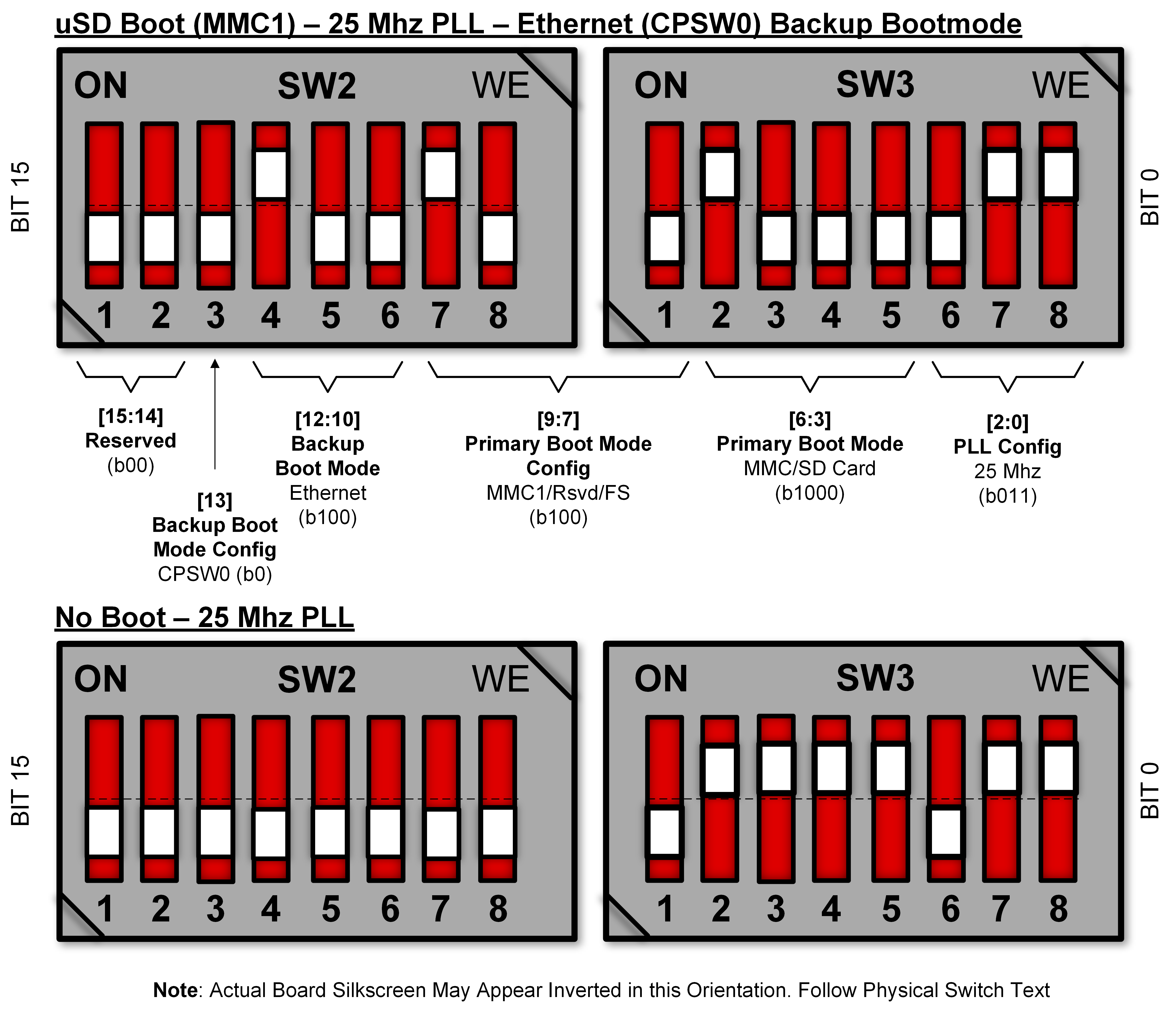
- Place the SK EVM boot switch
selectors (SW2, SW3) into selected boot mode. Example boot-modes for SD card and
no-boot are shown below. For additional options, see Section 4.4.4.1.
 Figure 4-4 Common Bootmode Switch
Positions
 - Connect your boot media (if applicable).
- Attach the 5 V USB Type-C cable to the SK EVM Type-C (J8) Connector.
- Connect the other end of the Type-C cable to the source, either AC Power Adapter, or Type C source device (such as a Laptop computer).
- Use ON/OFF sliding switch SW5 to Power on the board.
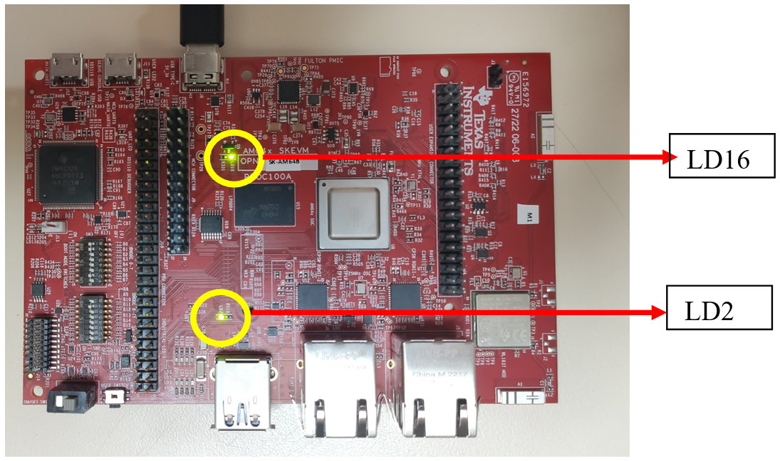
- Visually inspect the LEDs against the
reference photos below. The following LEDs are illuminated: LD2 and LD16 on top side
of the board.
 Figure 4-5 Top LED
 - XDS110 JTAG and UART debug console
output are routed to micro-USB ports J12 and J11, respectively. Note: Linux console output is routed to the second enumerated ttyUSB port.