SPRUIY9B May 2021 – October 2023
- 1
- Abstract
- Trademarks
- 1Key Features
- 2EVM Revisions and Assembly Variants
- 3Important Usage Notes
-
4System Description
- 4.1 Key Features
- 4.2 Functional Block Diagram
- 4.3 Power-On/Off Procedures
- 4.4
Peripheral and Major Component
Description
- 4.4.1 Clocking
- 4.4.2 Reset
- 4.4.3 Power
- 4.4.4 Configuration
- 4.4.5 JTAG
- 4.4.6 Test Automation
- 4.4.7 UART Interface
- 4.4.8 Memory Interfaces
- 4.4.9 Ethernet Interface
- 4.4.10 USB 3.0 Interface
- 4.4.11 PRU Connector
- 4.4.12 User Expansion Connector
- 4.4.13 MCU Connector
- 4.4.14 Interrupt
- 4.4.15 I2C Interface
- 4.4.16 IO Expander (GPIOs)
-
5Known Issues
- 5.1 Issue 1: LP8733x Max output Capacitance Spec Exceeded on LDO0 and LDO1
- 5.2 Issue 2: LP8733x Output Voltage of 0.9V Exceeds AM64x VDDR_CORE max Voltage Spec of 0.895 V
- 5.3 Issue 3 - SDIO Devices on MMC0 Require Careful Trace Lengths to Meet Interface Timing Requirements
- 5.4 Issue 4 - LPDDR4 Data Rate Limitation in Stressful Conditions
- 5.5 Issue 5 - Junk Character
- 5.6 Issue 6 - Test Power Down Signal Floating
- 5.7 Issue 7 - uSD Boot Not Working
- 6Regulatory Compliance
- 7Revision History
4.4.1.1 Ethernet PHY Clock
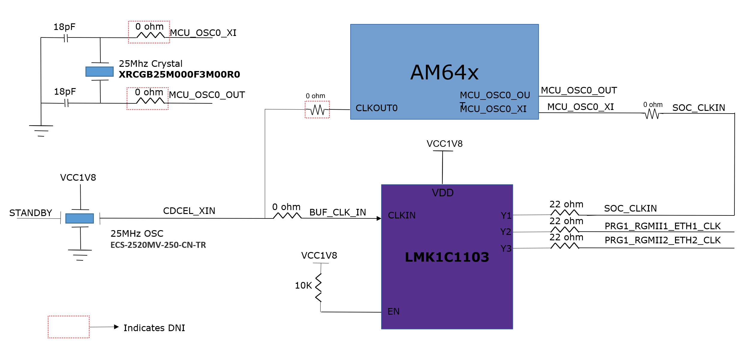
The clock buffer of part number LMK1C1103PWR is used to drive the 25 MHz clock to the Ethernet PHYs. LMK1C1103PWR is a 1:3 LVCMOS clock buffer, which takes a 25 MHz crystal/LVCMOS reference input and provides four 25 MHz LVCMOS clock outputs. The source for the clock buffer is either the CLKOUT0 pin from the SoC or a 25 MHz oscillator (ECS-2520MV-250-CN-TR). The selection can be made using a set of resistors. By default, the oscillator is used as input to the clock buffer in SK-AM64B EVM. Output Y2 and Y3 of the clock buffer LMK1C1103PWR are used as a reference clock input for two Gigabit Ethernet PHYs in SKEVM.
 Figure 4-6 AM64x SK EVM Clock
Tree