SPRUJ12F August 2021 – January 2024 AM2431 , AM2432 , AM2434
- 1
- Abstract
- Trademarks
- 1Preface: Read This First
- 2Kit Overview
- 3Board Setup
-
4Hardware Description
- 4.1 Functional Block Diagram
- 4.2 BoosterPack Headers
- 4.3 GPIO Mapping
- 4.4 Reset
- 4.5 Clock
- 4.6 Memory Interface
- 4.7 Ethernet Interface
- 4.8 USB 2.0 Interface
- 4.9 I2C Interface
- 4.10 Industrial Application LEDs
- 4.11 UART Interface
- 4.12 eQEP Interface
- 4.13 CAN Interface
- 4.14 FSI Interface
- 4.15 JTAG Emulation
- 4.16 Test Automation Interface
- 4.17 SPI Interface
- 5References
- A E3 Design Changes
- B Revision A Design Changes
- Revision History
4.14 FSI Interface
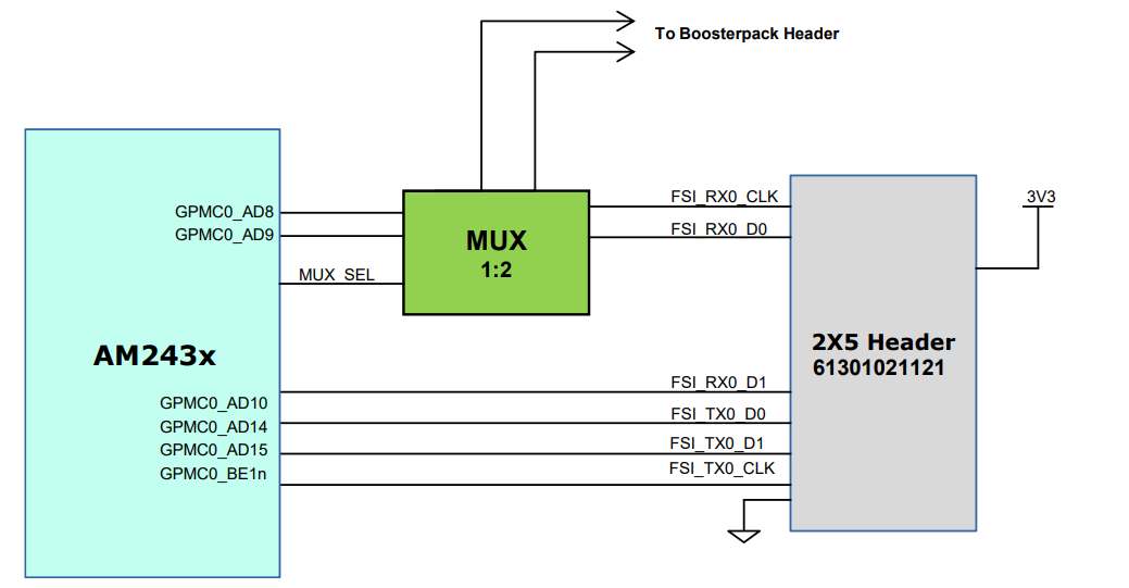
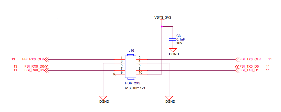
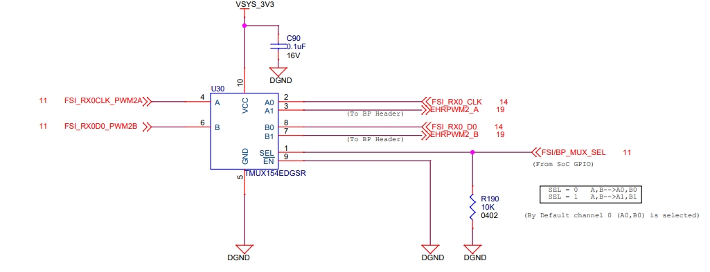
The LaunchPad supports one FSI Interface from the SoC that terminates to a 2x5 header (J16). The 2x5 header has a 3.3 V supply. A 1:2 active mux IC (TMUX154EDGSR) is used to interface the signals between the FSI header and the BoosterPack header as both the FSI and EHRPWM signals are internally muxed inside the SoC.
 Figure 4-23 FSI Interface
Table 4-19 FSI Header Pin
Description
| Pin Number | Signal |
|---|---|
| J16.1 | FSI_RX0_CLK |
| J16.2 | FSI_TX0_CLK |
| J16.3 | GND |
| J16.4 | GND |
| J16.5 | FSI_RX0_D0 |
| J16.6 | FSI_TX0_D0 |
| J16.7 | FSI_RX0_D1 |
| J16.8 | FSI_TX0_D1 |
| J16.9 | No connection |
| J16.10 | VSYS_3V3 |
 Figure 4-24 FSI Header
 Figure 4-25 FSI or BoosterPack Mux
Selection Circuit