SPRUJ22C November 2021 – September 2024 AWR2944 , AWR2944P
- 1
- Description
- Features
- 4
- 1Evaluation Module Overview
-
2Hardware
- 2.1 Block Diagram
- 2.2 PCB Handling Recommendations
- 2.3 Power Connections
- 2.4
Connectors
- 2.4.1 MIPI 60-Pin Connector (J19)
- 2.4.2 Debug Connector-60 pin (J7)
- 2.4.3 CAN-A Interface Connector (J3)
- 2.4.4 CAN-B Interface Connector (J2)
- 2.4.5 Ethernet Ports (J4 and J9)
- 2.4.6 USB Connectors (J8, J10)
- 2.4.7 OSC_CLKOUT Connector (J14)
- 2.4.8 PMIC SPI Connector (J16) (DNP)
- 2.4.9 Voltage Rails Ripple Measurement Connectors (J1, J5) (DNP)
- 2.5 Antenna
- 2.6 PMIC
- 2.7 On-Board Sensors
- 2.8 PC Connection
- 2.9 Connecting the AWR2944EVM/AWR2944PEVM to the DCA1000 EVM
- 2.10 Jumpers, Switches, and LEDs
- 3Software
- 4Hardware Design Files
- 5Compliance Information
- 6Additional Information
- 7Revision History
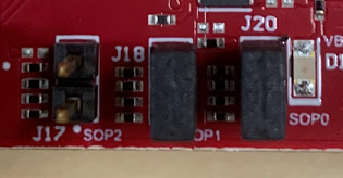
2.10.2 Sense On Power (SOP) Jumpers (J17, J18, J20)
The AWR2944EVM/AWR2944PEVM can be set to operate in different modes based on the state of the SOP [2:0] lines. These lines are sensed ONLY during boot up of the AWR2944 device. The state of the device is described in Table 2-12.
A closed jumper refers to a ‘1’ and open the jumper refers to a ‘0’ state of the SOP signal going to the AWR2944 device.
| Reference | Usage | Comments |
|---|---|---|
|
J17 (SOP 2), J18 (SOP 1), J20 (SOP 0) |
SOP[2:0] |
101 (SOP mode 5) = Flashing mode 001 (SOP mode 4) = Functional mode 000 (SOP mode 3) = Reserved 011 (SOP mode 2) = Development mode 010 (SOP mode 1) = Reserved |
 Figure 2-28 SOP Jumpers
Additionally, the SOP[4:3] signals defines the XTAL clock input as per the below configurations provided in Table 2-13.
| Reference | Usage | Comments |
|---|---|---|
|
R303, R312 Populated. R301,R309 unpopulated |
SOP[4:3] | 00 = 40MHz (Default state) |
|
R301, R312 Populated. R303,R319 unpopulated |
01 = 45.1584MHz | |
|
R303, R309 Populated. R301,R312 unpopulated |
10 = 49.152MHz | |
|
R301, R309 Populated. R303,R312 unpopulated |
11 = 50MHz |