SPRUJ40C may 2022 – may 2023
- 1
- Abstract
- Trademarks
- 1EVM Revisions and Assembly Variants
-
2System Description
- 2.1 Key Features
- 2.2 Functional Block Diagram (SK-AM62 and SK-AM62B)
- 2.3 Functional Block Diagram (SK-AM62-P1 and SK-AM62B-P1)
- 2.4 AM62x SKEVM Interface Mapping
- 2.5 Power ON/OFF Procedures
- 2.6
Peripheral and Major Component
Description
- 2.6.1 Clocking
- 2.6.2 Reset
- 2.6.3 OLDI Display Interface
- 2.6.4 CSI Interface
- 2.6.5 Audio Codec Interface
- 2.6.6 HDMI Display Interface
- 2.6.7 JTAG Interface
- 2.6.8 Test Automation Header
- 2.6.9 UART Interface
- 2.6.10 USB Interface
- 2.6.11 Memory Interfaces
- 2.6.12 Ethernet Interface
- 2.6.13 GPIO Port Expander
- 2.6.14 GPIO Mapping
- 2.6.15 Power
- 2.6.16 AM62x SKEVM User Setup/Configuration
- 2.6.17 Expansion Headers
- 2.6.18 Interrupt
- 2.6.19 I2C Address Mapping
-
3Known Issues and Modifications
- 3.1 Issue 1 - HDMI/DSS Incorrect Colors on E1
- 3.2 Issue 2 - J9 and J10 Header Alignment on E1
- 3.3 Issue 3 - USB Boot descoped on E1
- 3.4 Issue 4 - OLDI Connector Orientation and Pinout
- 3.5 Issue 5 - Bluetooth descoped on E2 EVMs
- 3.6 Issue 6 - Ethernet PHY CLK Skew Default Strapping Changes
- 3.7 Issue 7 - TEST_POWERDOWN changes
- 3.8 Issue 8 - MMC1_SDCD spurious interrupts
- 3.9 Issue 9 - PD Controller I2C2 IRQ Not Pinned Out
- 3.10 Issue 10 - INA Current Monitor Adress Changes
- 3.11 Issue 11 - Test Automation I2C Buffer Changes
- Regulatory Compliance
- Revision History
2.6.1 Clocking
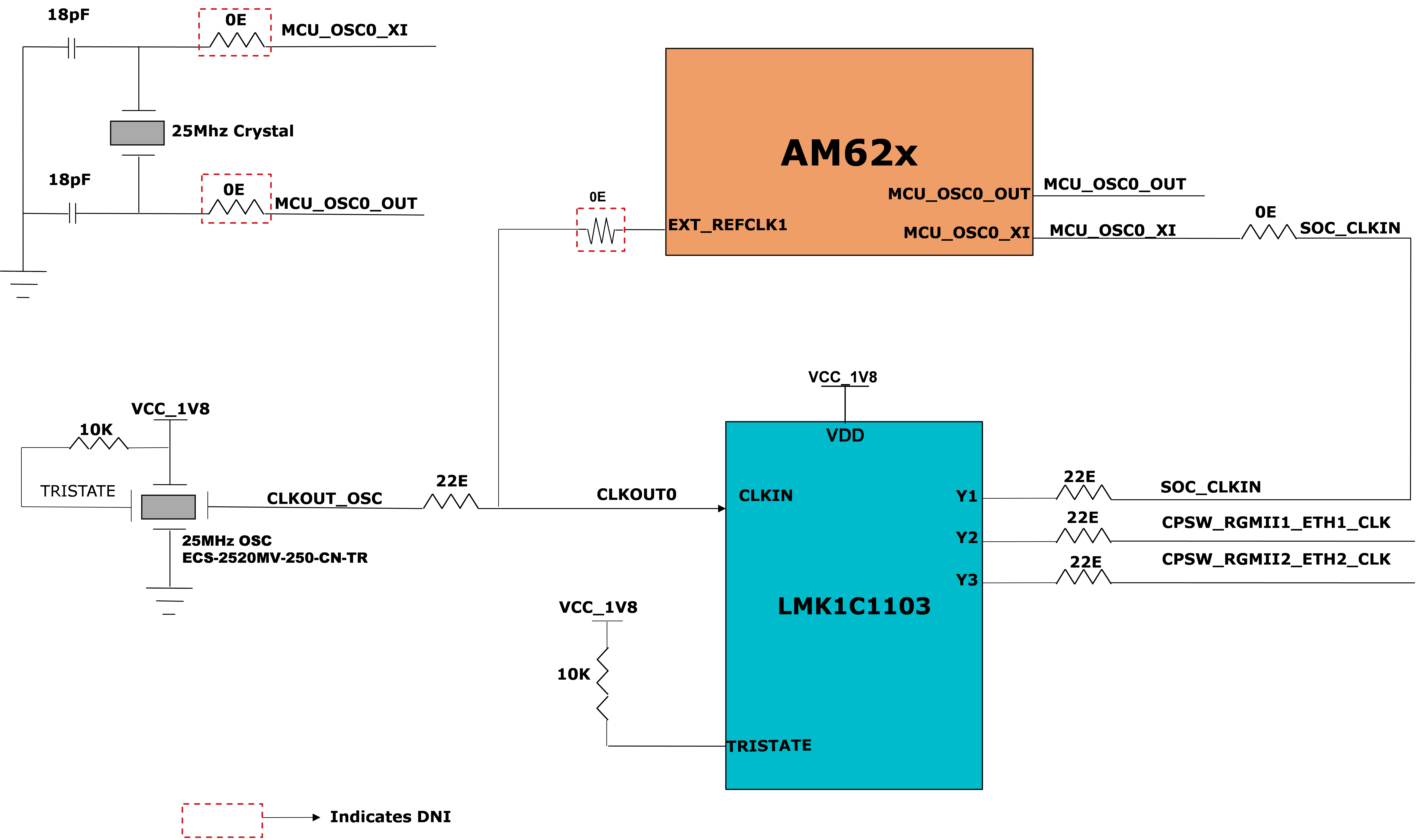
Figure 2-9 shows the clock architecture of AM62x SKEVM.
 Figure 2-9 Clock Architecture of
AM62x SKEVM
Figure 2-9 Clock Architecture of
AM62x SKEVMA clock generator of part number LMK1C1103PWR is used to drive the 25 MHz clock to the SoC and two Ethernet PHYs. LMK1C1103PWR is a 1:4 LVCMOS clock buffer, which takes the 25 MHz crystal/LVCMOS reference input and provides three 25 MHz LVCMOS clock outputs. The source for the clock buffer shall be either the CLKOUT0 pin from the SoC or a 25 MHz oscillator, the selection is made using a set of resistors. By default, an oscillator is used as input to the clock buffer on the AM62x SKEVM. Output Y2 and Y3 of the clock buffer are used as reference clock inputs] for two Gigabit Ethernet PHYs.
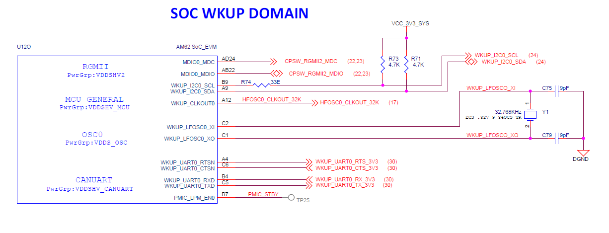
There is one external crystal attached to the AM62x SoC to provide clock to the WKUP domain of the SoC (32.768 KHz).
 Figure 2-10 SoC WKUP
Domain