SPRUJ66A February 2023 – December 2023
- 1
- Abstract
- Trademarks
- 1EVM Revisions and Assembly Variants
- 2Inside the Box
- 3EMC, EMI, and ESD Compliance
-
4System Description
- 4.1 Key Features
- 4.2 Functional Block Diagram
- 4.3 AM62A Low Power SK EVM Interface Mapping
- 4.4 Power ON/OFF Procedures
- 4.5
Peripheral and Major Component Description
- 4.5.1 Clocking
- 4.5.2 Reset
- 4.5.3 CSI Interface
- 4.5.4 Audio Codec Interface
- 4.5.5 HDMI Display Interface
- 4.5.6 JTAG Interface
- 4.5.7 Test Automation Header
- 4.5.8 UART Interface
- 4.5.9 USB Interface
- 4.5.10 Memory Interfaces
- 4.5.11 Ethernet Interface
- 4.5.12 GPIO Port Expander
- 4.5.13 GPIO Mapping
- 4.5.14 Power
- 4.5.15 AM62A Low Power SK EVM User Setup and Configuration
- 4.5.16 Expansion Headers
- 4.5.17 I2C Address Mapping
- 5Revision History
4.5.9.1 USB 2 0 Type A Interface
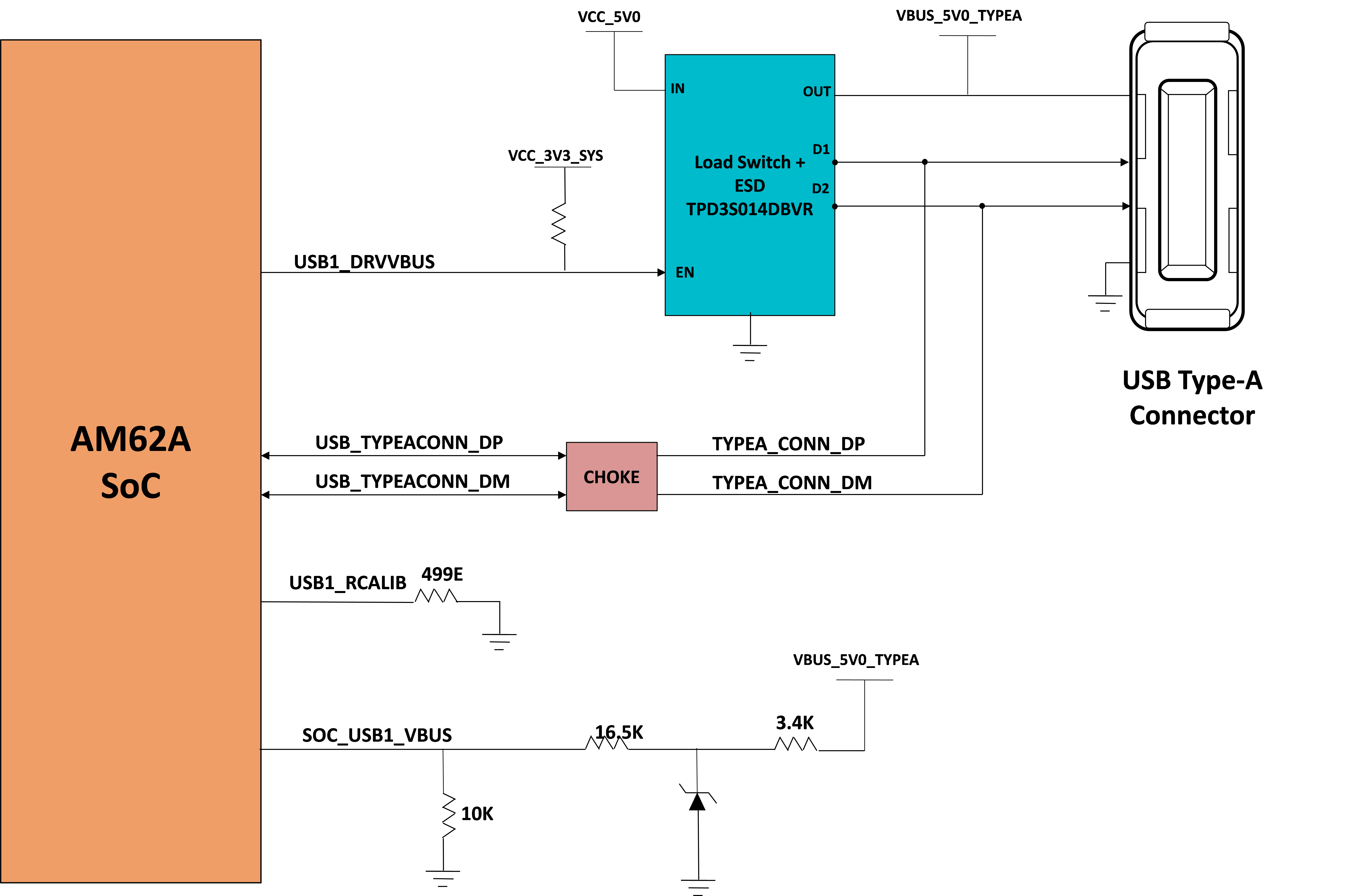
USB2.0 data lines from Type A connector J7 are connected to the USB1 interface of the AM62A SOC to provide USB high-speed/full-speed communication. USB1_VBUS to the SOC is provided through a resistor divider network to support (5V-30V) VBUS operation. USB1_DRVVBUS from SOC is connected to the enable pin of Load switch Mfr Part # TPD3S014DBVR to allow on board 5V supply to power the VBUS.
A common mode choke of Mfr Part# DLW21SZ900HQ2B is provided on USB Data lines for EMI/ EMC reduction.USB Data lines from Type-A connectors are also connected to the Current Limit Load Switch and ESD Protection IC Mfr Part# TPD3S014DBVR. This switch limits the current to 500mA and dissipates the ESD strikes above the maximum level specified in the IEC 61000-4-2.
 Figure 4-18 USB Type A interface block diagram