SPRUJ66A February 2023 – December 2023
- 1
- Abstract
- Trademarks
- 1EVM Revisions and Assembly Variants
- 2Inside the Box
- 3EMC, EMI, and ESD Compliance
-
4System Description
- 4.1 Key Features
- 4.2 Functional Block Diagram
- 4.3 AM62A Low Power SK EVM Interface Mapping
- 4.4 Power ON/OFF Procedures
- 4.5
Peripheral and Major Component Description
- 4.5.1 Clocking
- 4.5.2 Reset
- 4.5.3 CSI Interface
- 4.5.4 Audio Codec Interface
- 4.5.5 HDMI Display Interface
- 4.5.6 JTAG Interface
- 4.5.7 Test Automation Header
- 4.5.8 UART Interface
- 4.5.9 USB Interface
- 4.5.10 Memory Interfaces
- 4.5.11 Ethernet Interface
- 4.5.12 GPIO Port Expander
- 4.5.13 GPIO Mapping
- 4.5.14 Power
- 4.5.15 AM62A Low Power SK EVM User Setup and Configuration
- 4.5.16 Expansion Headers
- 4.5.17 I2C Address Mapping
- 5Revision History
4.5.6 JTAG Interface
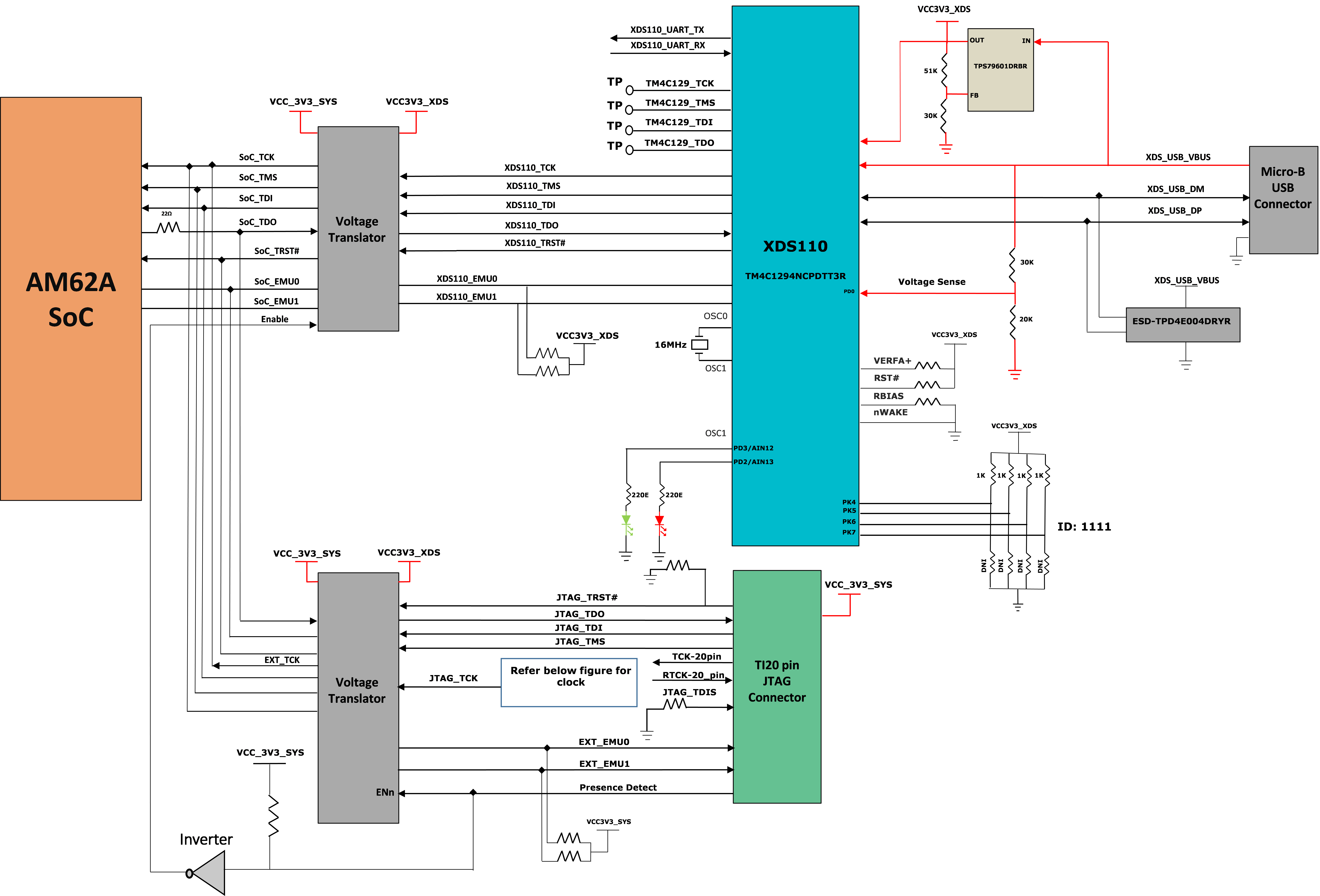
The AM62A Low Power SK EVM board includes XDS110 class on board emulation. The connection for this emulator uses an USB 2.0 micro-B connector and the circuit acts as a Bus powered USB device. The VBUS power from the connector is used to power the emulation circuit such that connection to the emulator is not lost when the power to the SKEVM is removed. Voltage translation buffers are used to isolate the XDS110 circuit from the rest of the SKEVM.
Optionally, the JTAG Interface on SKEVM is also provided through a 20 Pin Standard JTAG cTI Header J19. This allows the user to connect an external JTAG Emulator Cable. Voltage translation buffers are used to isolate the JTAGsignals of cTI header from the rest of the SKEVM. The output of the voltage translators from XDS110 Section and cTI Header Section are muxed and connected to the AM62A JTAG Interface. If a connection to the cTI 20 Pin JTAG connector is sensed using an auto presence detect circuit, the mux routes the 20 pin signals from the cTI connector to the AM62A SoC in place of the on-board emulation circuit.
 Figure 4-15 JTAG Interface block diagram
The pin-out of the cTI 20 pin JTAG connector are given in the table below. A ESD protection part number TPD4E004 is provided on USB signals to steer ESD current pulses to VCC or GND. TPD4E004 protects against ESD pulses up to ±15-kV Human-Body Model (HBM) as specified in IEC 61000-4-2 and provides ±8-kV contact discharge and ±12- kV air-gap discharge.
| Pin No. | Signal |
| 1 | JTAG_TMS |
| 2 | JTAG_TRST# |
| 3 | JTAG_TDI |
| 4 | JTAG_TDIS |
| 5 | VCC_3V3_SYS |
| 6 | NC |
| 7 | JTAG_TDO |
| 8 | SEL_XDS110_INV |
| 9 | JTAG_cTI_RTCK |
| 10 | DGND |
| 11 | JTAG_cTI_TCK |
| 12 | DGND |
| 13 | JTAG_EMU0 |
| 14 | JTAG_EMU1 |
| 15 | JTAG_EMU_RSTn |
| 16 | DGND |
| 17 | NC |
| 18 | NC |
| 19 | NC |
| 20 | DGND |