SPRUJ73 December 2023
2.5.5.3 NOR FLASH
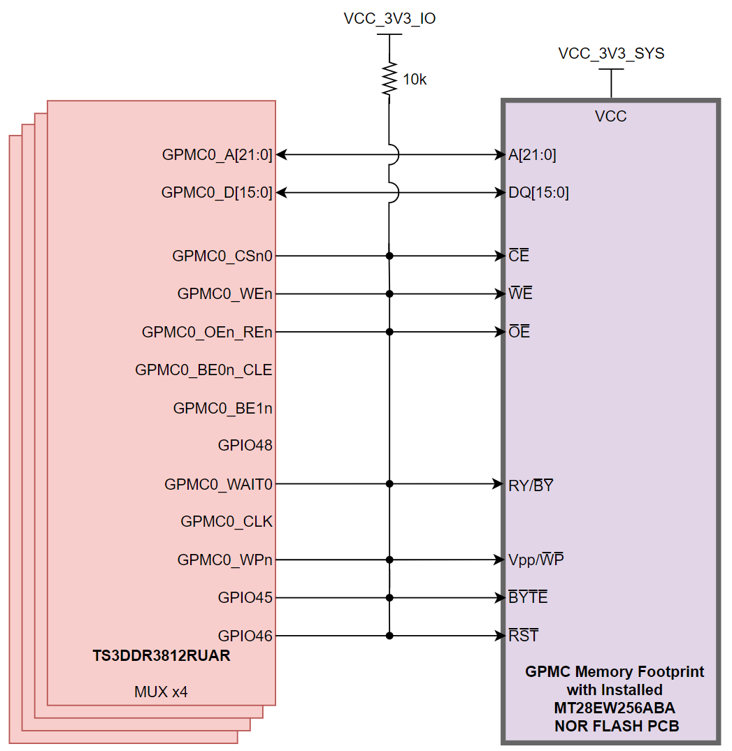
The AM263x controlCARD Docking Station design package includes a design for a custom PCB with a MT28EW256ABA NOR FLASH memory module mounted on it. This enables a user to develop using the GPMC0 interface of the AM263x SoC with a NOR FLASH memory module.
 Figure 2-14 GPMC-NOR FLASH
Interface
Figure 2-14 GPMC-NOR FLASH
InterfaceThe GPMC signals originating from the AM263x SoC are passed through the HSEC connector onto the Docking Station. The TRACE/GPMC multiplexing scheme sends the GPMC signals to the GPMC memory footprint, and onto the installed custom MT28EW256ABA NOR FLASH PCB. Refer to Table 3-14 for details on the MUX scheme operation.
All select and enable signals are to be pulled high via 10 kΩ resistors to ensure functionality of the active low signals.
| AM263x Signal | MT28EW256ABA NOR FLASH Signal | ||
|---|---|---|---|
| GPMC0_A[21:0] | GPMC Address Output | A[MAX:0] | Address |
| GPMC0_AD[15:0] | GPMC Data Input/Output | DQ[15:0] | Data I/O |
| GPMC0_CSn0 | GPMC Chip Select 0 (active low) | C̅E̅ | Chip Enable |
| GPMC0_WEn | GPMC Write Enable (active low) | W̅E̅ | Write Enable |
| GPMC0_OEn_REn | GPMC Output Enable (active low) or Read Enable (active low) | O̅E̅ | Output Enable |
| GPMC0_BE0n_CLE | GPMC Lower-Byte Enable (active low) or Command Latch Enable | N/A | N/A |
| GPMC0_BE1n | GPMC Upper-Byte Enable (active low) | N/A | N/A |
| GPMC0_WAIT0 | GPMC External Indication of Wait | RY/B̅Y̅ | Ready busy |
| GPMC0_WPn | GPMC Flash Write Protect (active low) | Vpp/W̅P̅ | Vpp/Write Protect |
| GPIO45 | General-Purpose IO 45 | B̅Y̅T̅E̅ | Byte/word organization select |
| GPIO46 | General-Purpose IO 46 | R̅S̅T̅ | Reset |
| GPIO48 | General-Purpose IO 48 | N/A | N/A |