SPRUJ85A April 2024 – August 2024
PRODUCTION DATA
- 1
- Description
- 1Key Features
- 2LaunchPad Module Overview
-
3Hardware Description
- 4.1 Board Setup
- 4.2 Functional Block Diagram
- 4.3 GPIO Mapping
- 4.4 Reset
- 4.5 Clock
- 4.6 Memory Interfaces
- 4.7 Ethernet Interface
- 4.8 I2C
- 4.9 Industrial Application LEDs
- 4.10 SPI
- 4.11 UART
- 4.12 MCAN
- 4.13 FSI
- 4.14 JTAG
- 4.15 TIVA and Test Automation Header
- 4.16 LIN
- 4.17 ADC and DAC
- 4.18 EQEP and SDFM
- 4.19 EPWM
- 4.20 BoosterPack Headers
- 4.21 Pinmux Mapping
- 4Additional Information
- 5References
- 6Revision History
3.1.3 Boot mode Selection
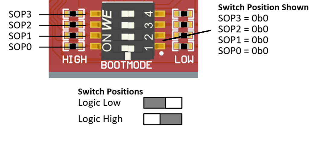
The boot mode for the AM263Px is selected by a DIP (Dual In-Line Package) switch (SW1) or the test automation header. The test automation header uses an I2C expansion buffer to drive the boot mode when PORz is toggled. The supported boot modes are shown in Table 3-6. The DIP Switch configurations for each boot mode are shown in Table 3-5.

Figure 3-6 Boot mode DIP Switch Positions - LP AM263Px E2 SW1 SOP Switches
| Boot mode | SPI0_D0_pad (SOP3 - SW1.4) | SPI0_CLK_pad (SOP2 - SW1.3) | QSPI_D1 (SOP1 - SW1.2) | QSPI_D0 (SOP0 - SW1.1) |
|---|---|---|---|---|
| OSPI (4S) - Quad Read Mode | 1 | 1 | 1 | 1 |
| UART | 1 | 1 | 1 | 0 |
| OSPI (1S) - Single Read Mode | 1 | 1 | 0 | 1 |
| OSPI (8S) - Octal Read Mode | 1 | 1 | 0 | 0 |
| DevBoot | 0 | 1 | 0 | 0 |
| xSPI 8D (SFDP) | 0 | 0 | 1 | 1 |
| Unsupported boot mode | All other combinations not defined above | |||
| Boot mode/Peripheral | Boot Media/Host | Notes |
|---|---|---|
| OSPI (4S) - Quad Read Mode | OSPI Flash |
Download and boot SBL from OSPI flash in quad read mode. Attempt Primary SBL, followed by Secondary SBL if primary loading fails. |
| UART | External Host |
Download and boot SBL from UART interface via XMODEM protocol at 115200bps BaudRate. |
| OSPI (1S) - Single Read Mode | OSPI Flash |
Download and boot SBL from OSPI flash in single read mode. Attempt Primary SBL, followed by Secondary SBL if primary loading fails. |
| OSPI (8S) - Octal Read Mode | OSPI Flash |
Download and boot SBL from OSPI flash in octal read mode. Attempt Primary SBL, followed by Secondary SBL if primary loading fails. |
| xSPI 8D (SFDP) | OSPI Flash |
Read SFDP table for read command, download and boot SBL from OSPI flash in 8D mode. Attempt Primary SBL, followed by Secondary SBL if primary loading fails. |
| DevBoot | N/A | No SBL. Used for development purposes only. |