SPRUJ86C October 2023 – August 2024 AM263P2 , AM263P4 , AM263P4-Q1
- 1
- Description
- Features
- 4
- 1Evaluation Module Overview
-
2Hardware
- 2.1 Component Identification
- 2.2 Power Requirements
- 2.3 Functional Block Diagram
- 2.4 Reset
- 2.5 Clock
- 2.6 Boot Mode Selection
- 2.7 JTAG Path Selection
- 2.8 Header Information
- 2.9 GPIO Mapping
- 2.10 Push Buttons
- 2.11 Interfaces
- 2.12 HSEC Pinout and Pinmux Mapping
- 3Hardware Design Files
- 4Additional Information
- 5Related Documentation
- 6References
- 7Revision History
- 8Revision History
2.11.13 ADC and DAC
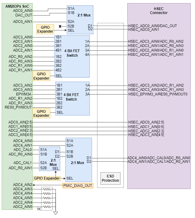
The AM263Px Control Card supports 24 ADC signal channels that are mapped for the AM263Px SoC and terminated to the HSEC connector. All ADC signals are ESD protected (TPD4E001DBVR).
 Figure 2-35 ADC HSEC Connections
There are two muxes (TMUX1136DQAR) that determine the pathing of ADC signals to and from the HSEC Connector.
Table 2-28 ADC MUX Select Logic
| MUX Select Signal | Condition | Function | Description |
|---|---|---|---|
| ADC1_MUX_SEL | SEL Signal HIGH | S1A → D1 | HSEC_ADC0_AIN0 selected |
| S2A → D2 | HSEC_ADC0_AIN1 selected | ||
| SEL Signal LOW | S1B → D1 | HSEC_DAC_OUT selected | |
| S2B → D2 | HSEC_DAC_OUT selected | ||
| ADC2_MUX_SEL | SEL Signal HIGH | S1A → D1 | HSEC_ADC4_AIN0 selected |
| S2A → D2 | HSEC_ADC4_AIN1 selected | ||
| SEL Signal LOW | S1B → D1 | ADC_CAL0 selected | |
| S2B → D2 | ADC_CAL1 selected |
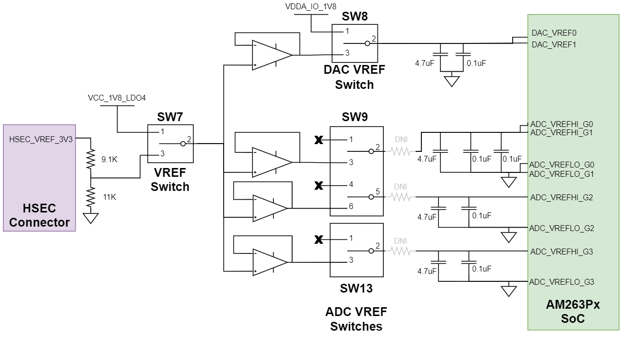
There are three switches that are used to configure the reference voltages for the ADC and DAC.
 Figure 2-36 ADC Switch Routing
- The VREF Switch (SW7) is a single
pole double throw switch that controls which 1.8V reference is used for ADC and
DAC.Table 2-29 VREF Switch
VREF Switch Position Reference Selection Pin 1-2 On board 1.8V Reference (REF3318AIDBZT) Pin 2-3 HSEC VREF - The DAC
VREF Switch (SW8) is a single pole double throw switch that controls the input
for the DAC VREF inputs of the AM263Px SoC.Table 2-30 DAC VREF Switch
DAC VREF Switch Position Reference Selection Pin 1-2 AM263Px on-die LDO Pin 2-3 Output of VREF Switch - The ADC VREF Switch (SW9)
contains two single pole double throw switches that control the input for the
ADC VREF inputs of the AM263Px SoC.Note: SW9.1 must be in the Pin 1-2 position and SW9.2 must be in the pin 4-5 position for AM263Px MCU+ SDK ADC Examples to function properly.Table 2-31 ADC VREF Switch
ADC VREF Switch Position Reference Selection Pin 1-2 OPEN - Allow for reference to be AM263Px on-die LDO reference Pin 2-3 Output of VREF Switch Pin 4-5 OPEN - Allow for reference to be AM263Px on-die LDO reference Pin 5-6 Output of VREF Switch