SPRUJ93 august   2023


  1.   1
  2.   Description
  3.   Features
  4.   4
  5. 1Evaluation Module Overview
    1.     Preface: Read This First
      1. 1.1.1 Sitara™ MCU+ Academy
      2. 1.1.2 If You Need Assistance
      3. 1.1.3 Important Usage Notes
    2. 1.1 Introduction
    3. 1.2 Kit Contents
    4. 1.3 Specification
    5. 1.4 Device Information
    6. 1.5 HSEC 180-pin Control Card Docking Station
    7. 1.6 Security
  6. 2Hardware
    1. 2.1  Functional Block Diagram
    2. 2.2  Component Identification
    3. 2.3  Power Requirements
      1. 2.3.1 Power Input Using USB Type-C Connector
      2. 2.3.2 Power Status LEDs
      3. 2.3.3 Power Tree
      4. 2.3.4 Power Sequence
      5. 2.3.5 PMIC
    4. 2.4  Reset
    5. 2.5  Clock
    6. 2.6  Boot Mode Selection
    7. 2.7  JTAG Path Selection
    8. 2.8  Header Information
    9. 2.9  GPIO Mapping
    10. 2.10 Push Buttons
    11. 2.11 Test Points
    12. 2.12 Interfaces
      1. 2.12.1  Memory Interface
        1. 2.12.1.1 QSPI
        2. 2.12.1.2 Board ID EEPROM
      2. 2.12.2  Ethernet Interface
        1. 2.12.2.1 RGMII
        2. 2.12.2.2 PRU-ICSS
        3. 2.12.2.3 LED Indication in RJ45 Connector
      3. 2.12.3  I2C
      4. 2.12.4  Industrial Application LEDs
      5. 2.12.5  SPI
      6. 2.12.6  UART
      7. 2.12.7  MCAN
      8. 2.12.8  FSI
      9. 2.12.9  JTAG
      10. 2.12.10 Test Automation Header
      11. 2.12.11 LIN
      12. 2.12.12 MMC
      13. 2.12.13 ADC and DAC
    13. 2.13 HSEC Pinout and Pinmux Mapping
  7. 3Software
    1. 3.1 SDK Installation
  8. 4Hardware Design Files
  9. 5Additional Information
    1. 5.1 Trademarks
    2. 5.2 E1 Design Hardware Modifications
  10. 6References
    1. 6.1 Reference Documents
    2. 6.2 Other TI Components Used in This Design

QSPI

The AM263x Control Card has a 128 Mbit QSPI memory device (S25FL128SAGNFI000), which is connected to the QSPI0 interface of the AM263x SoC. The QSPI supports single data rates with memory speeds up to 104 MHz. The QSPI flash is powered by the 3.3-V IO supply (VSYS_3V3A).

Note: There is typically a reset pin for flash memory. The reset pin is not present in the WSON package that is used in the Control Card.

The QSPI0_D0/D1 signals are also used for BOOTMODE control logic. There are 10-kΩ resistors used to isolate the BOOTMODE control logic after the value is latched.
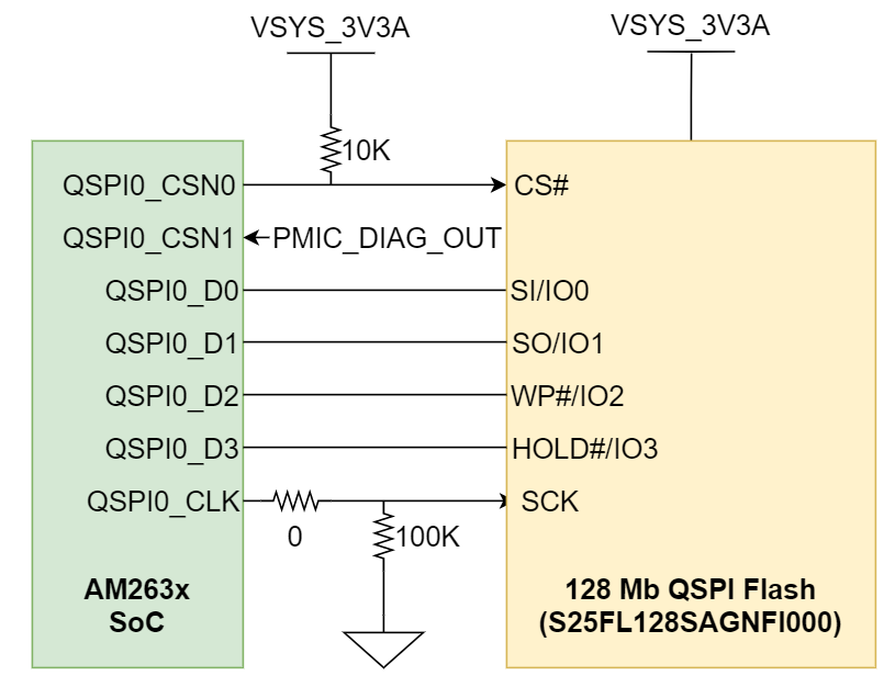
GUID-20230515-SS0I-KK98-3GBC-FWK3F1LMKJTP-low.png Figure 2-16 QSPI