SPRUJ93 august 2023
- 1
- Description
- Features
- 4
- 1Evaluation Module Overview
-
2Hardware
- 2.1 Functional Block Diagram
- 2.2 Component Identification
- 2.3 Power Requirements
- 2.4 Reset
- 2.5 Clock
- 2.6 Boot Mode Selection
- 2.7 JTAG Path Selection
- 2.8 Header Information
- 2.9 GPIO Mapping
- 2.10 Push Buttons
- 2.11 Test Points
- 2.12 Interfaces
- 2.13 HSEC Pinout and Pinmux Mapping
- 3Software
- 4Hardware Design Files
- 5Additional Information
- 6References
2.12.2.1 RGMII
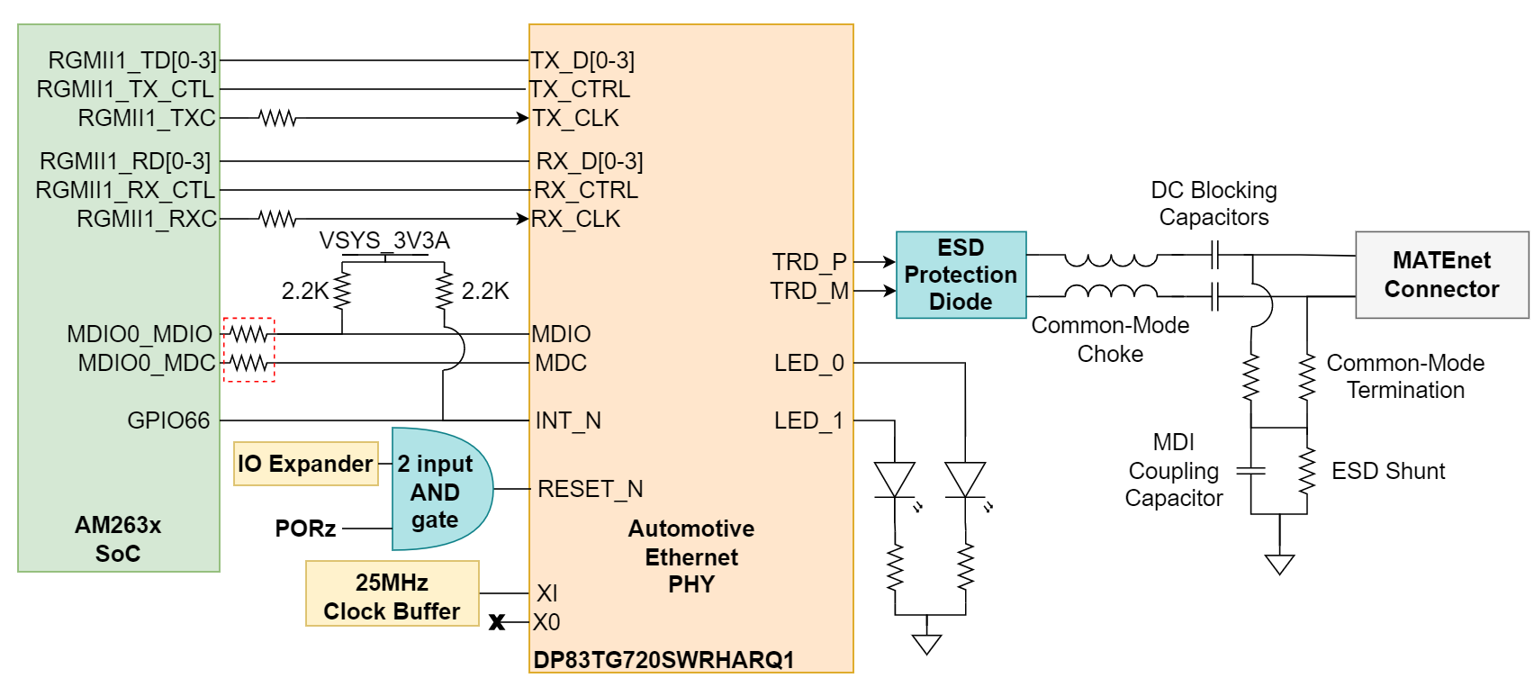
The AM263x Control Card uses one port of RGMII signals to be connected to a 48-pin Ethernet PHY (DP83TG730SWRHARQ1). The PHY is configured to advertise 1-Gb operation. The Ethernet data signals of the PHY are terminated to a MATEnet Connector. LEDs are used to indicate link status and activity.
 Figure 2-18 RGMII1 Automotive Ethernet PHY
The Ethernet PHY requires three separate power sources. VSYS_3V3A from the PMIC is filtered using two different ferrite beads to supply voltage to VDDIO and VDDA of the Ethernet PHY. There is a dedicated LDO for the 1.0 V supply for the Ethernet PHY.
There are series termination resistors on the transmit and receive clock signals located near the AM263x SoC.
The MDIO and interrupt signals from the SoC to the PHY require 2.2 kΩ pull up resistors to the I/O supply voltage for proper operation. The interrupt signal is driven by a GPIO signal that is mapped from the AM263x SoC.
The reset signal for the Ethernet PHY is driven by a 2-input AND gate. The AND gate's inputs are a GPIO signal that is generated by the IO Expander and PORz.
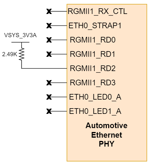
The Ethernet PHY uses many functional pins as strap option to place the device into specific modes of operation.
 Figure 2-19 RGMII1 Automotive Ethernet PHY
Strapping Resistors
Figure 2-19 RGMII1 Automotive Ethernet PHY
Strapping Resistors| Functional Pin | Default Mode | Mode in CC | Function |
|---|---|---|---|
| RX_D0 | 0 | 0 | RGMII (Align Mode) |
| RX_D1 | 0 | 0 | |
| RX_D2 | 0 | 1 | |
| RX_CTRL | 0 | 0 | PHY Address: 0x0000 |
| STRP_1 | 0 | 0 | |
| LED_0 | 0 | 0 | MS: Peripheral |
| LED_1 | 0 | 0 | AUTO: Autonomous |