SPRUJ93 august 2023
- 1
- Description
- Features
- 4
- 1Evaluation Module Overview
-
2Hardware
- 2.1 Functional Block Diagram
- 2.2 Component Identification
- 2.3 Power Requirements
- 2.4 Reset
- 2.5 Clock
- 2.6 Boot Mode Selection
- 2.7 JTAG Path Selection
- 2.8 Header Information
- 2.9 GPIO Mapping
- 2.10 Push Buttons
- 2.11 Test Points
- 2.12 Interfaces
- 2.13 HSEC Pinout and Pinmux Mapping
- 3Software
- 4Hardware Design Files
- 5Additional Information
- 6References
2.12.12 MMC
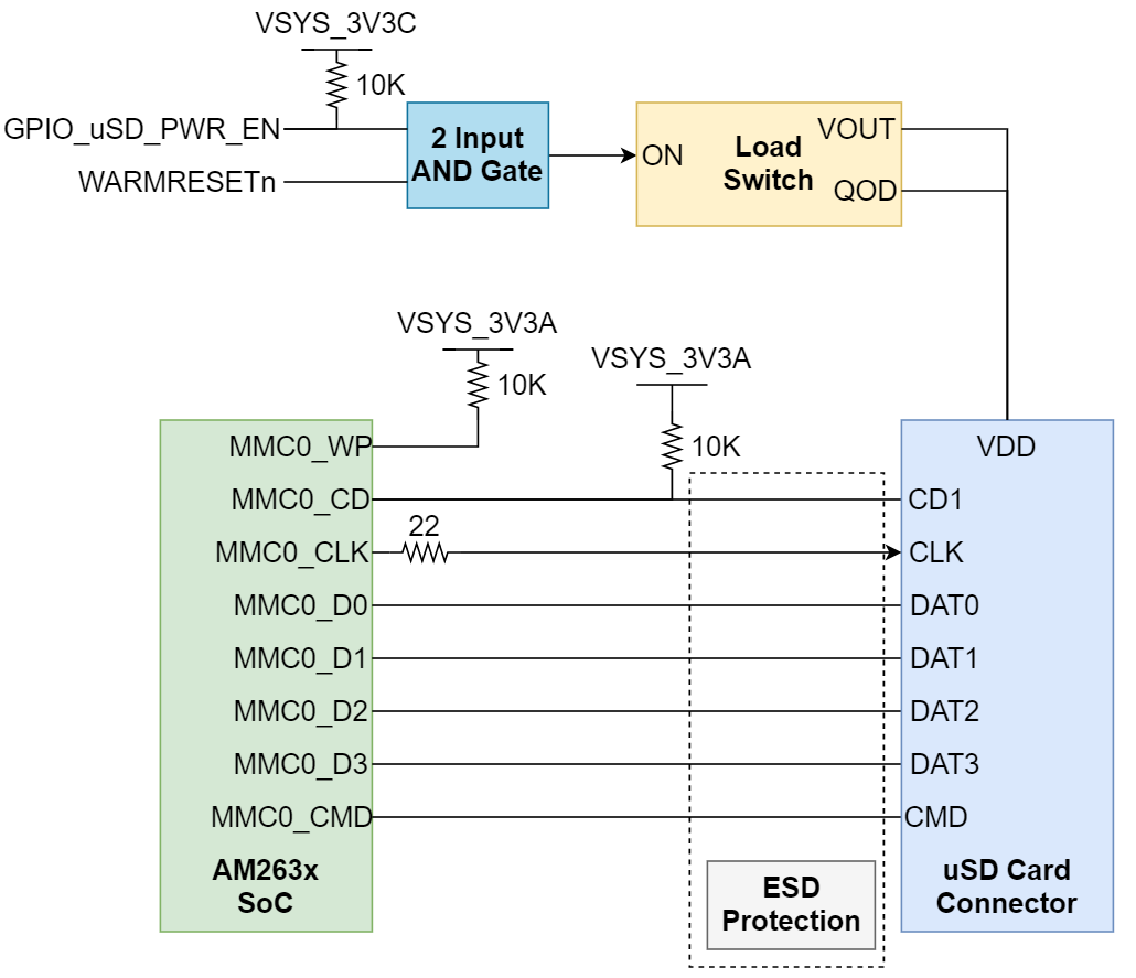
The AM263x Control Card provides a micro SD card interface that is mapped to the MMC0 instance of the AM263x SoC.
 Figure 2-34 Micro-SD Connector Interface
A load switch (TPS22918DBVR) is used to power the micro SD card connector. The load switch is driven by the output of a 2-input AND gate between WARMRESETn and GPIO_uSD_PWR_EN to power cycle the card upon reset. The load switch uses quick output discharge (QOD) to make sure that the supply voltage reaches <10% of nominal value during reset.
Inline ESD protection is provided for the MMC signals in the form of a six channel transient voltage suppressor device (TPD6E001RSER).
The Write Protect (WP) and Card Detect (CD) signals of the SD card connector are pulled up to the 3.3 V IO voltage supply.
A series termination resistor is provided for the MMC clock signal.