SPRUJ93 august 2023
- 1
- Description
- Features
- 4
- 1Evaluation Module Overview
-
2Hardware
- 2.1 Functional Block Diagram
- 2.2 Component Identification
- 2.3 Power Requirements
- 2.4 Reset
- 2.5 Clock
- 2.6 Boot Mode Selection
- 2.7 JTAG Path Selection
- 2.8 Header Information
- 2.9 GPIO Mapping
- 2.10 Push Buttons
- 2.11 Test Points
- 2.12 Interfaces
- 2.13 HSEC Pinout and Pinmux Mapping
- 3Software
- 4Hardware Design Files
- 5Additional Information
- 6References
2.5 Clock
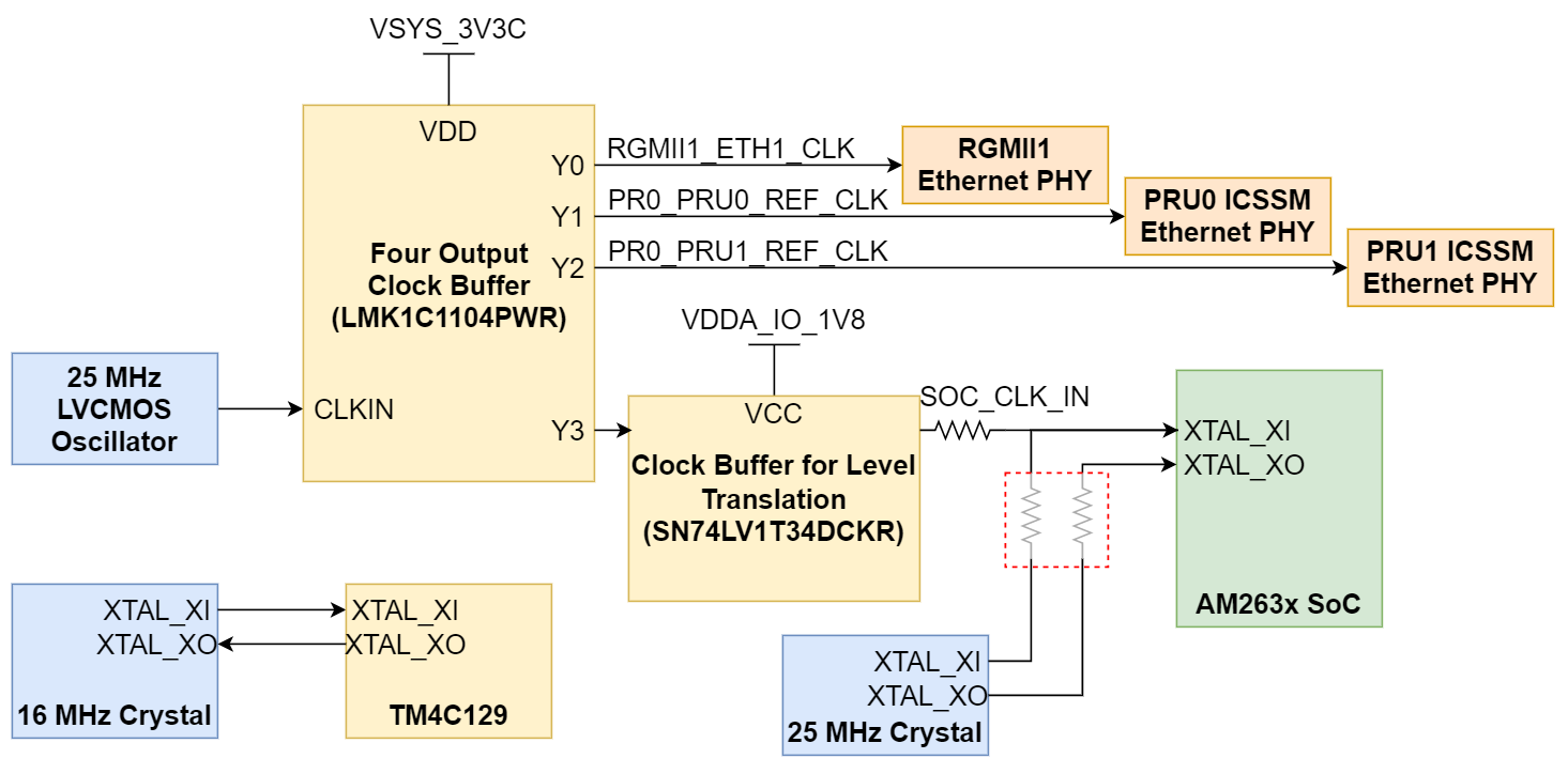
The AM263x SoC requires a 25-MHz clock input for XTAL_XI. All reference clocks required for the SoC and the three Ethernet PHYs are generated from a single four output clock buffer (LMK1C1104PWR), which is sourced from a single 25-MHz LVCMOS Oscillator by default. A clock buffer is used for level translation from 3.3 V to 1.8 V.
The Control Card also requires a 16-MHz clock source for the TM4C129 microcontroller for UART-USB JTAG support.

Alternatively, the SoC clock input can be sourced from a single 25-MHz crystal. To use the crystal there must be resistors mounted and unmounted as shown in Table 3-3. When the using a crystal as the SoC clock source, then the AM263x CLKOUT0 signal is used to source the four output clock buffer for the Ethernet PHY reference clock signals.
 Figure 2-13 Crystal Clock Tree
The following table describes the proper resistors to be mounted and DNI'd for each clock source configuration.
| Clock Source | Mounted | DNI |
|---|---|---|
| 25-MHz LVCMOS Oscillator (default) | R161, R135 | R158, R155, R134 |
| 25-MHz Crystal | R158, R155, R134 | R161, R135 |