SPRUJ93 august 2023
- 1
- Description
- Features
- 4
- 1Evaluation Module Overview
-
2Hardware
- 2.1 Functional Block Diagram
- 2.2 Component Identification
- 2.3 Power Requirements
- 2.4 Reset
- 2.5 Clock
- 2.6 Boot Mode Selection
- 2.7 JTAG Path Selection
- 2.8 Header Information
- 2.9 GPIO Mapping
- 2.10 Push Buttons
- 2.11 Test Points
- 2.12 Interfaces
- 2.13 HSEC Pinout and Pinmux Mapping
- 3Software
- 4Hardware Design Files
- 5Additional Information
- 6References
2.12.7 MCAN
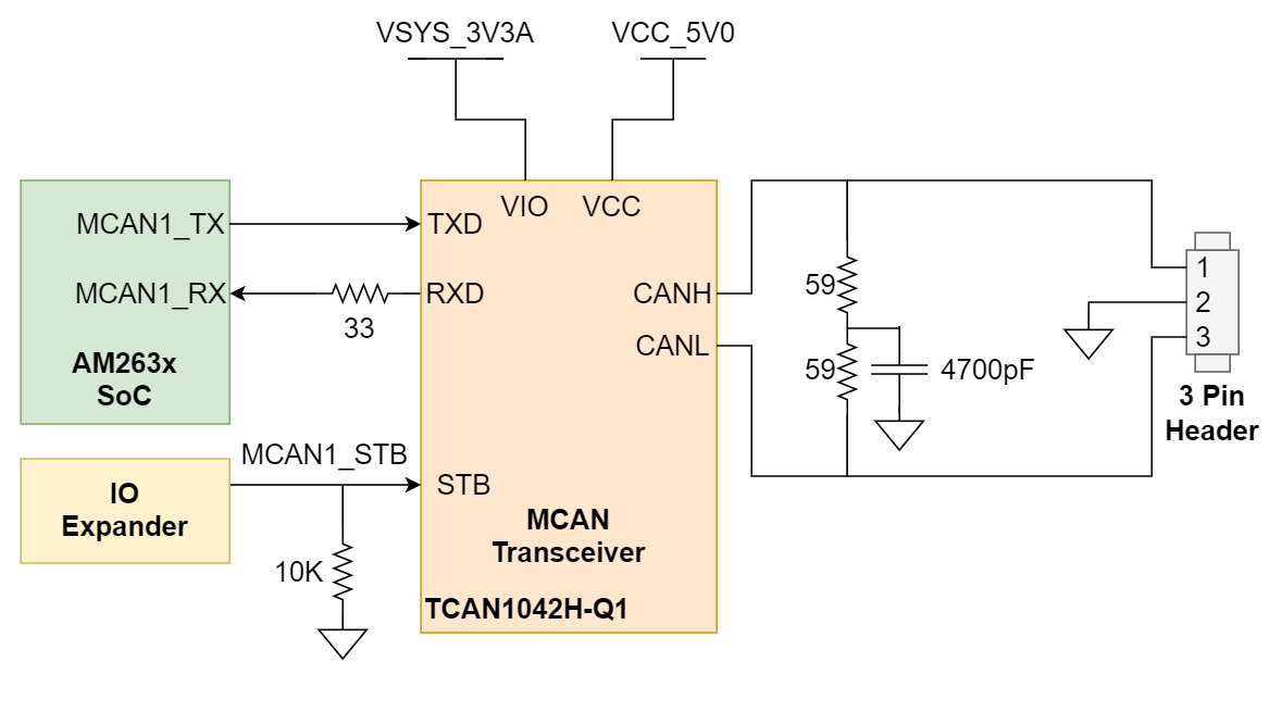
The Control Card is equipped with a single MCAN transceiver (TCAN1024H-Q1) that is connected to the MCAN1 interface of the AM263x SoC. The MCAN0 interface of the AM263x SoC is mapped directly to the HSEC connector.
 Figure 2-28 MCAN Transceiver
The MCAN transceiver has two power inputs, VIO is the transceiver I/O level shifting supply voltage and VCC is the transceiver 5 V supply voltage. The SoC CAN data transmit data input is mapped to TXD of the transceiver and the CAN receive data output of the transceiver is mapped to the MCAN RX signal of the SoC with a series termination resistor close to the transceiver.
The standby control signal is a GPIO signal sourced from the IO expander. The STB control input is active high and a pulldown resistor is used to have the transceiver operate in normal mode as opposed to the standby mode that is default due to a weak internal pull up.
The system has a 120 Ω split termination on the CANH and CANL signals to improve EMI performance. Split termination improves the electromagnetic emissions behavior of the network by eliminating fluctuations in the bus common-mode voltages at the start and end of message transmissions.
The low- and high-level CAN bus input output lines are terminated to a three pin header.