SPRUJ93 august 2023
- 1
- Description
- Features
- 4
- 1Evaluation Module Overview
-
2Hardware
- 2.1 Functional Block Diagram
- 2.2 Component Identification
- 2.3 Power Requirements
- 2.4 Reset
- 2.5 Clock
- 2.6 Boot Mode Selection
- 2.7 JTAG Path Selection
- 2.8 Header Information
- 2.9 GPIO Mapping
- 2.10 Push Buttons
- 2.11 Test Points
- 2.12 Interfaces
- 2.13 HSEC Pinout and Pinmux Mapping
- 3Software
- 4Hardware Design Files
- 5Additional Information
- 6References
5.2 E1 Design Hardware Modifications
The following section describes the hardware modifications that were made to each E1 Control Card.
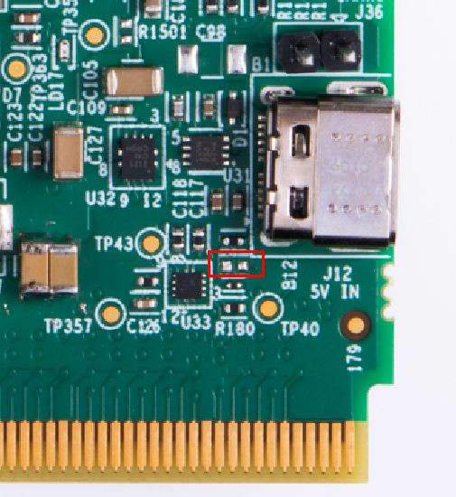
- TUSB320 CC Controller GPIO Mode
- The TUSB320 is intended to be used in the GPIO mode to negotiate whether the type-C CC pins represent a power source that is an excellent choice for the Control Card. For the TUSB320 to be GPIO mode, the ADDR pin needs to floating and therefore R170 was removed.
- Modification 1:
- Depopulate R170
 Figure 5-1 Modification 1
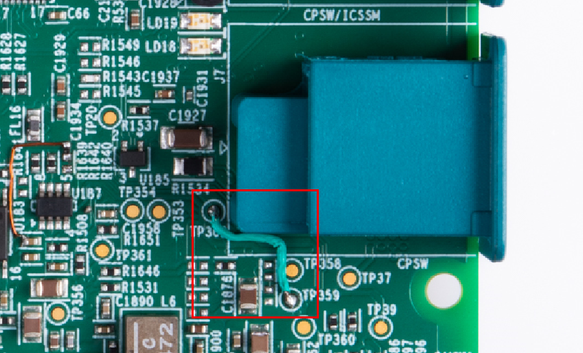
- Bypass PMIC VSYS_3V3C Power
- The PMIC LDO output VSOUT2 is used to power the VSYS_3V3C power net. VSYS_3V3C is used to power loads for various peripheral circuits, many of which are required for AM263x reset and boot.
- The PMIC LDO output VSOUT2 is disabled by default and requires a SPI register write from the AM263x to enable after initial start-up.
- As a workaround, the VSYS_3V3C rail is shorted with the VSYS_3V3A PMIC output.
- Modification 2:
- Lift pin U30.29 from PMIC to disconnect LDO output of PMIC
- Short TP359 and TP362 using 22GA wire
 Figure 5-2 Modification 2
- TPS37042A30 Startup RESET Output Transients
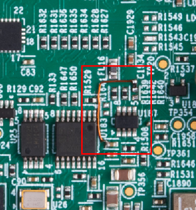
- The TPS37042A3O power supervisor (U187) open-drain outputs RESET1# and RESET2# cause transient PORZ assertions during initial 3.3V (VSYS_3V3A) and 1.2V (VSYS_1V2) power-on.
- These open-drain outputs are pulled to USB-C/HSEC supplied VMAIN 5.0V supply. That VMAIN supply showed noisy behavior during start-up and caused these open-drain I/O to provide a faulty PORZ. Changing U187 RESET1# and RESET2# output pull-up resistors to reference PMIC supplied VDD_5V0 creates a functional PORZ.
- Modification 3:
- Remove R1640
- Install 10 kΩ pull-up resistor on the RESET# output pad of the R1640 resistor position
- Attach the other 10 kΩ resistor pad to the VDD_5V0 power net
 Figure 5-3 Modification 3