SPRUJA1 October   2023


  1.   1
  2.   Description
  3.   Get Started
  4.   Features
  5.   5
  6. 1Evaluation Module Overview
    1. 1.1 Introduction
    2. 1.2 Kit Contents
    3. 1.3 Specification
    4. 1.4 Device Information
  7. 2Hardware
    1. 2.1  Additional Images
    2. 2.2  Key Features
      1. 2.2.1 Processor
      2. 2.2.2 Power Supply
      3. 2.2.3 Memory
      4. 2.2.4 JTAG/Emulator
      5. 2.2.5 Support Interfaces and Peripherals
      6. 2.2.6 Expansion Connectors/Headers
    3. 2.3  Interface Mapping
    4. 2.4  Power ON/OFF Procedure
      1. 2.4.1 Power ON Procedure
      2. 2.4.2 Power OFF Procedure
      3. 2.4.3 Power Test Points
    5. 2.5  Clocking
      1. 2.5.1 Peripheral Ref Clock
    6. 2.6  Reset
    7. 2.7  CSI Interface
    8. 2.8  Audio Codec Interface
    9. 2.9  HDMI Display Interface
    10. 2.10 JTAG Interface
    11. 2.11 Test Automation Header
    12. 2.12 UART Interface
    13. 2.13 USB Interface
      1. 2.13.1 USB 2.0 Type A Interface
      2. 2.13.2 USB 2.0 Type C Interface
    14. 2.14 Memory Interfaces
      1. 2.14.1 OSPI Interface
      2. 2.14.2 MMC Interfaces
        1. 2.14.2.1 MMC0 - eMMC Interface
        2. 2.14.2.2 MMC1 - Micro SD Interface
        3. 2.14.2.3 MMC2 - M.2 Key E Interface
      3. 2.14.3 Board ID EEPROM
    15. 2.15 Ethernet Interface
      1. 2.15.1 CPSW Ethernet PHY 1 Default Configuration
      2. 2.15.2 CPSW Ethernet PHY 2 Default Configuration
    16. 2.16 GPIO Port Expander
    17. 2.17 GPIO Mapping
    18. 2.18 OLDI Display Interface
    19. 2.19 Power
      1. 2.19.1 Power Requirements
      2. 2.19.2 Power Input
      3. 2.19.3 Power Supply
      4. 2.19.4 Power Sequencing
      5. 2.19.5 AM62x SIP SoC Power
      6. 2.19.6 Current Monitoring
    20. 2.20 EVM User Setup/Configuration
      1. 2.20.1 EVM DIP Switches
      2. 2.20.2 Boot Modes
      3. 2.20.3 User Test LEDs
    21. 2.21 Expansion Headers
      1. 2.21.1 PRU Connector
      2. 2.21.2 User Expansion Connector
      3. 2.21.3 MCU Connector
    22. 2.22 Interrupt
    23. 2.23 I2C Address Mapping
  8. 3Hardware Design Files
  9. 4Compliance Information
    1. 4.1 Compliance and Certifications
  10. 5Additional Information
    1. 5.1 Trademarks

Additional Images

This section shows the EVM pictures and the location of various blocks on the board.
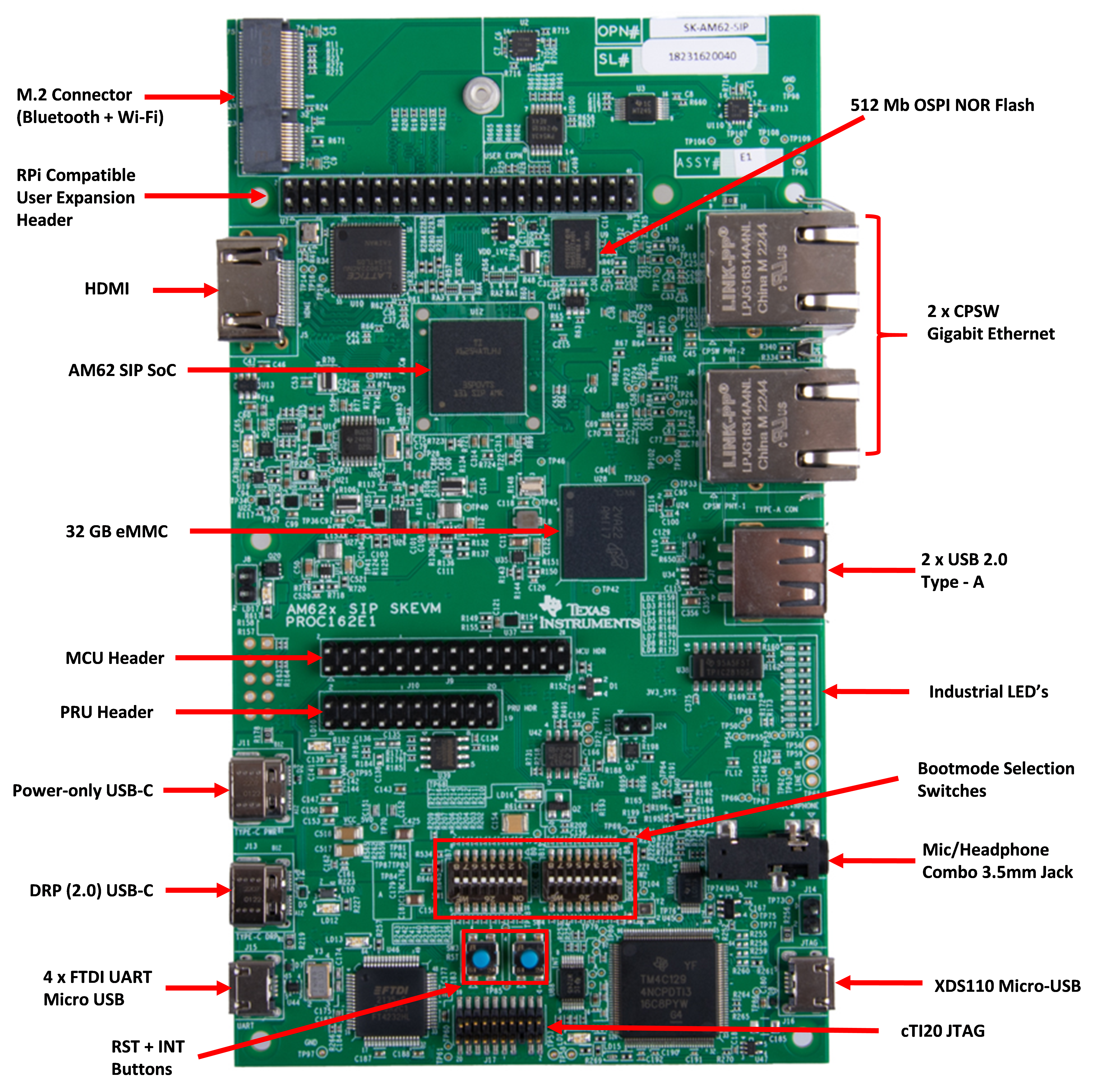
GUID-20231011-SS0I-ZKGC-5WZ8-RFCNHTWGLLBQ-low.png Figure 2-1 EVM Top Side
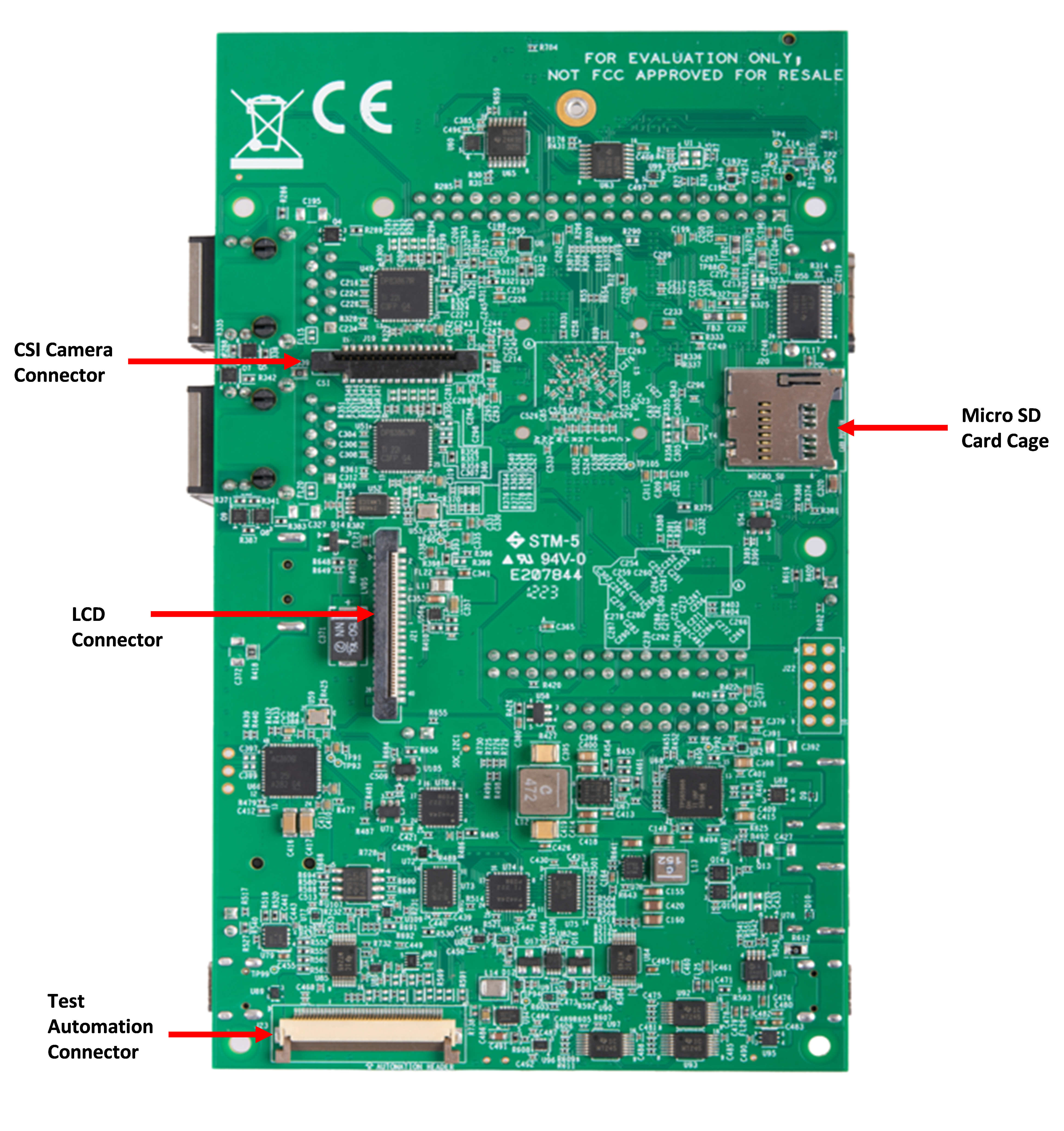
GUID-20231011-SS0I-70FK-RRWP-XFRVRB6X19DQ-low.png Figure 2-2 EVM Bottom Side