SPRUJA1 October 2023
- 1
- Description
- Get Started
- Features
- 5
- 1Evaluation Module Overview
-
2Hardware
- 2.1 Additional Images
- 2.2 Key Features
- 2.3 Interface Mapping
- 2.4 Power ON/OFF Procedure
- 2.5 Clocking
- 2.6 Reset
- 2.7 CSI Interface
- 2.8 Audio Codec Interface
- 2.9 HDMI Display Interface
- 2.10 JTAG Interface
- 2.11 Test Automation Header
- 2.12 UART Interface
- 2.13 USB Interface
- 2.14 Memory Interfaces
- 2.15 Ethernet Interface
- 2.16 GPIO Port Expander
- 2.17 GPIO Mapping
- 2.18 OLDI Display Interface
- 2.19 Power
- 2.20 EVM User Setup/Configuration
- 2.21 Expansion Headers
- 2.22 Interrupt
- 2.23 I2C Address Mapping
- 3Hardware Design Files
- 4Compliance Information
- 5Additional Information
2.11 Test Automation Header
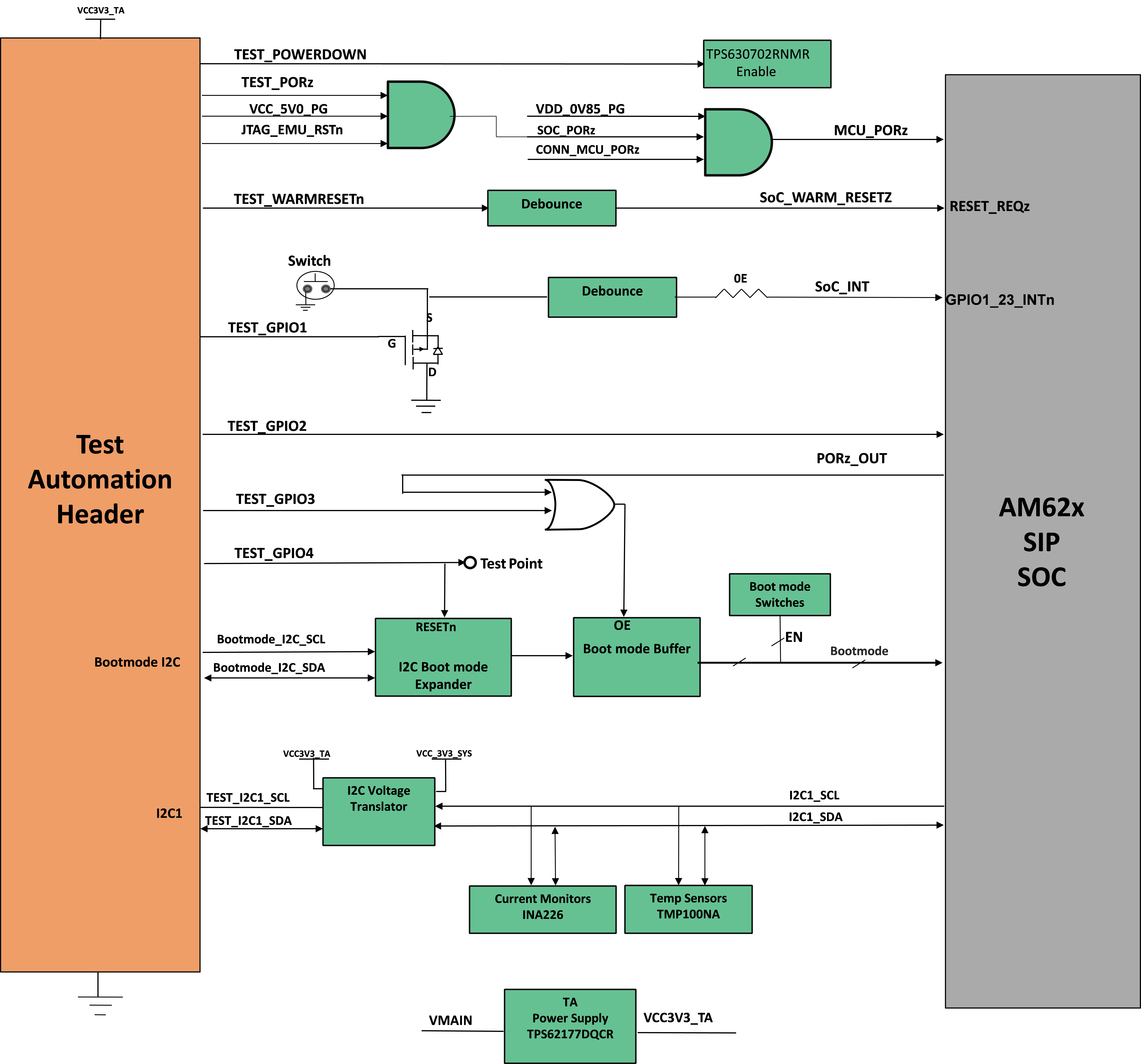
AM62x SIP SK EVM has a 40-pin test automation header (FH12A-40S-0.5SH) to allow an external controller to manipulate some basic operations like Power Down, POR, Warm Reset, Boot Mode control, and so forth.
The Test Automation Circuit is powered by the 3.3 V supply generated by a dedicated regulator Mfr. Part# TPS62177DQCR. The SoC’s I2C1 is connected to the test automation header. Another I2C instance (BOOTMODE_I2C) from the Test Automation Header is connected to the 24-bit I2C boot mode IO Expander of Mfr. Part# TCA6424ARGJR to allow control of the boot modes for the AM62x SIP SoC.
The test automation circuit has voltage translation circuits so that the controller is isolated from the IO voltages used by the AM62x SIP. Boot mode for the AM62x SIP must be controlled by either the user using DIP Switches or the test automation header through the I2C IO Expander. Boot Mode Buffers are used to isolate the Boot Mode controls driven through DIP Switches or I2C IO Expander. The boot mode is controlled by the user using two 8-bit DIP switches on the board, which connects a pull-up resistor to the output of a buffer when the switch is set to the ON position and to weaker pull-down resistor when set to the OFF position. The output of the buffer is connected to the boot mode pins on the AM62x SIP SoC and the output is enabled when the boot mode is needed during a reset cycle.
When boot mode is to be set through Test Automation header, the required switch values are set at the I2C IO expander output, which overwrites the DIP switch values to give the desired boot values to the SoC. The pins used for boot mode also have other functions which is isolated by disabling the boot mode buffer during normal operation.
The power down signal from the Test automation header instructs the SK EVM to power down all the rails except for dedicated power supplies on the board. Similarly PORZn signal is also provided to give a hard reset to the SoC and WARM_RESETn for warm reset of the SoC. One Interrupt signal from the Test Automation header is routed to the SoC GPIO (GPIO1_23) to provide an external Interrupt.
 Figure 2-11 Test Automation
| Pin No. | Signal | IO Direction | Pin No. | Signal | IO Direction |
|---|---|---|---|---|---|
| 1 | VCC3V3_TA | Power | 21 | NC | NA |
| 2 | VCC3V3_TA | Power | 22 | NC | NA |
| 3 | VCC3V3_TA | Power | 23 | NC | NA |
| 4 | NC | NA | 24 | NC | NA |
| 5 | NC | NA | 25 | DGND | Power |
| 6 | NC | NA | 26 | TEST_POWERDOWN | Input |
| 7 | DGND | Power | 27 | TEST_PORz | Input |
| 8 | NC | NA | 28 | TEST_WARMRESETn | Input |
| 9 | NC | NA | 29 | NC | NA |
| 10 | NC | NA | 30 | TEST_GPIO1 | Bidirectional |
| 11 | NC | NA | 31 | TEST_GPIO2 | Bidirectional |
| 12 | NC | NA | 32 | TEST_GPIO3 | Input |
| 13 | NC | NA | 33 | TEST_GPIO4 | Input |
| 14 | NC | NA | 34 | DGND | Power |
| 15 | NC | NA | 35 | NC | NA |
| 16 | DGND | Power | 36 | SoC_I2C1_TA_SCL | Bidirectional |
| 17 | NC | NA | 37 | BOOTMODE_I2C_SCL | Bidirectional |
| 18 | NC | NA | 38 | SoC_I2C1_TA_SDA | Bidirectional |
| 19 | NC | NA | 39 | BOOTMODE_I2C_SDA | Bidirectional |
| 20 | NC | NA | 40 | DGND | Power |