SPRUJA2 November   2023


  1.   1
  2.   Description
  3.   Get Started
  4.   Features
  5.   5
  6. 1Evaluation Module Overview
    1. 1.1 Introduction
    2. 1.2 Kit Contents
    3. 1.3 Device Information
    4. 1.4 Specification
  7. 2Hardware
    1. 2.1  Additional Images
    2. 2.2  Key Features
      1. 2.2.1 Processor
      2. 2.2.2 Power Supply
      3. 2.2.3 Memory
      4. 2.2.4 JTAG/Emulator
      5. 2.2.5 Supported Interfaces and Peripherals
      6. 2.2.6 Expansion Connectors/Headers
    3. 2.3  Interface Mapping
    4. 2.4  Power ON/OFF Procedure
      1. 2.4.1 Power ON Procedure
      2. 2.4.2 Power OFF Procedure
      3. 2.4.3 Test Points
    5. 2.5  Clocking
      1. 2.5.1 Peripheral Ref Clock
    6. 2.6  Reset
    7. 2.7  CSI Interface
    8. 2.8  OLDI Interface
    9. 2.9  DSI Interface
    10. 2.10 Audio Codec Interface
    11. 2.11 HDMI Display Interface
    12. 2.12 JTAG Interface
    13. 2.13 Test Automation Header
    14. 2.14 UART Interface
    15. 2.15 USB Interface
      1. 2.15.1 USB 2.0 Type A Interface
      2. 2.15.2 USB 2.0 Type C Interface
    16. 2.16 Memory Interfaces
      1. 2.16.1 LPDDR4 Interface
      2. 2.16.2 OSPI Interface
      3. 2.16.3 MMC Interfaces
        1. 2.16.3.1 MMC0 - eMMC Interface
        2. 2.16.3.2 MMC1 - Micro SD Interface
        3. 2.16.3.3 MMC2 - M.2 Key E Interface
      4. 2.16.4 Board ID EEPROM
    17. 2.17 Ethernet Interface
      1. 2.17.1 CPSW Ethernet PHY Strapping
      2. 2.17.2 CPSW Ethernet PHY1 Default Configuration
      3. 2.17.3 CPSW Ethernet PHY2 Default Configuration
    18. 2.18 GPIO Port Expander
    19. 2.19 GPIO Mapping
    20. 2.20 Power
      1. 2.20.1 Power Requirement
      2. 2.20.2 Power Input
      3. 2.20.3 Power Supply
      4. 2.20.4 Power Sequencing
      5. 2.20.5 AM62P SoC Power
      6. 2.20.6 Current Monitoring
    21. 2.21 EVM User Setup/Configuration
      1. 2.21.1 DIP Switches
      2. 2.21.2 Boot Modes
      3. 2.21.3 User Test LEDs
    22. 2.22 Expansion Headers
      1. 2.22.1 User Expansion Connector
      2. 2.22.2 MCU Connector
      3. 2.22.3 GPMC NAND (x8) Connector
    23. 2.23 Interrupt
    24. 2.24 I2C Address Mapping
  8. 3Hardware Design Files
  9. 4Compliance Information
    1. 4.1 Compliance and Certifications
  10. 5Additional Information
    1. 5.1 Known Hardware or Software Issues
      1. 5.1.1 Issue 1 - Watchdog Reset
      2. 5.1.2 Issue 2 - Power Down Sequence
    2. 5.2 Trademarks

Clocking

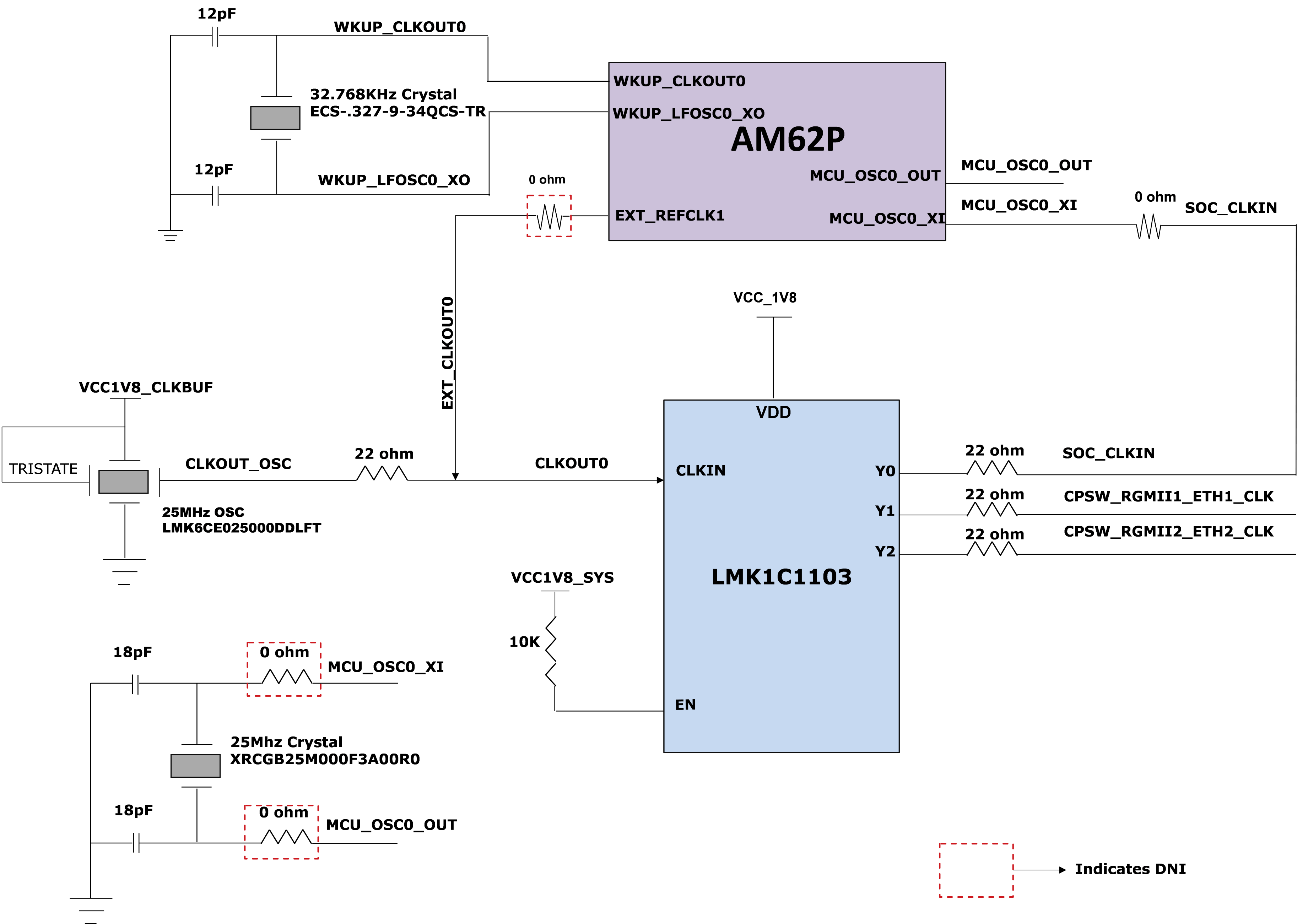
The clock architecture of AM62P SK EVM is shown below.
GUID-20231102-SS0I-390B-TSQG-T8DJBLDDHSTR-low.png Figure 2-4 Clock Architecture

A clock buffer of part number LMK1C1103PWR is used to drive the 25 MHz clock to the SOC and the two Ethernet PHYs. LMK1C1103PWR is a 1:3 LVCMOS clock buffer, which takes the 25 MHz crystal/LVCMOS reference input and provides three 25 MHz LVCMOS clock outputs. The source for the clock buffer shall be either the CLKOUT0 pin from the SOC or a 25 MHz oscillator, the selection of which is made using a set of resistors. By default, an oscillator is used as an input to the clock buffer on the AM62P SK EVM. Outputs Y1 and Y2 of the clock buffer are used as reference clock inputs for the two Gigabit Ethernet PHYs.

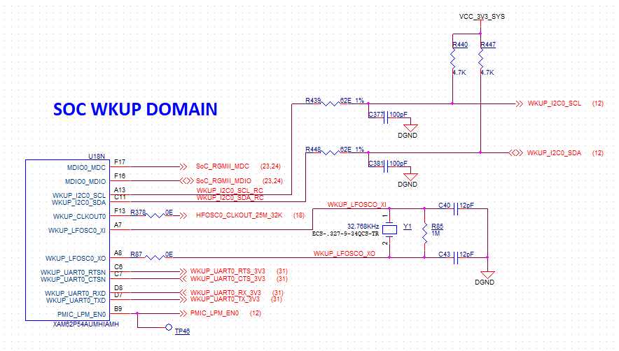
There is one external crystal (32.768 KHz) attached to the AM62P SOC to provide clock to the WKUP domain.
GUID-20231024-SS0I-T7DD-MK1Z-XBMFZ8XC1MC2-low.png Figure 2-5 SoC WKUP Domain Clock