SPRUJA2 November 2023
- 1
- Description
- Get Started
- Features
- 5
- 1Evaluation Module Overview
-
2Hardware
- 2.1 Additional Images
- 2.2 Key Features
- 2.3 Interface Mapping
- 2.4 Power ON/OFF Procedure
- 2.5 Clocking
- 2.6 Reset
- 2.7 CSI Interface
- 2.8 OLDI Interface
- 2.9 DSI Interface
- 2.10 Audio Codec Interface
- 2.11 HDMI Display Interface
- 2.12 JTAG Interface
- 2.13 Test Automation Header
- 2.14 UART Interface
- 2.15 USB Interface
- 2.16 Memory Interfaces
- 2.17 Ethernet Interface
- 2.18 GPIO Port Expander
- 2.19 GPIO Mapping
- 2.20 Power
- 2.21 EVM User Setup/Configuration
- 2.22 Expansion Headers
- 2.23 Interrupt
- 2.24 I2C Address Mapping
- 3Hardware Design Files
- 4Compliance Information
- 5Additional Information
2.15.2 USB 2.0 Type C Interface
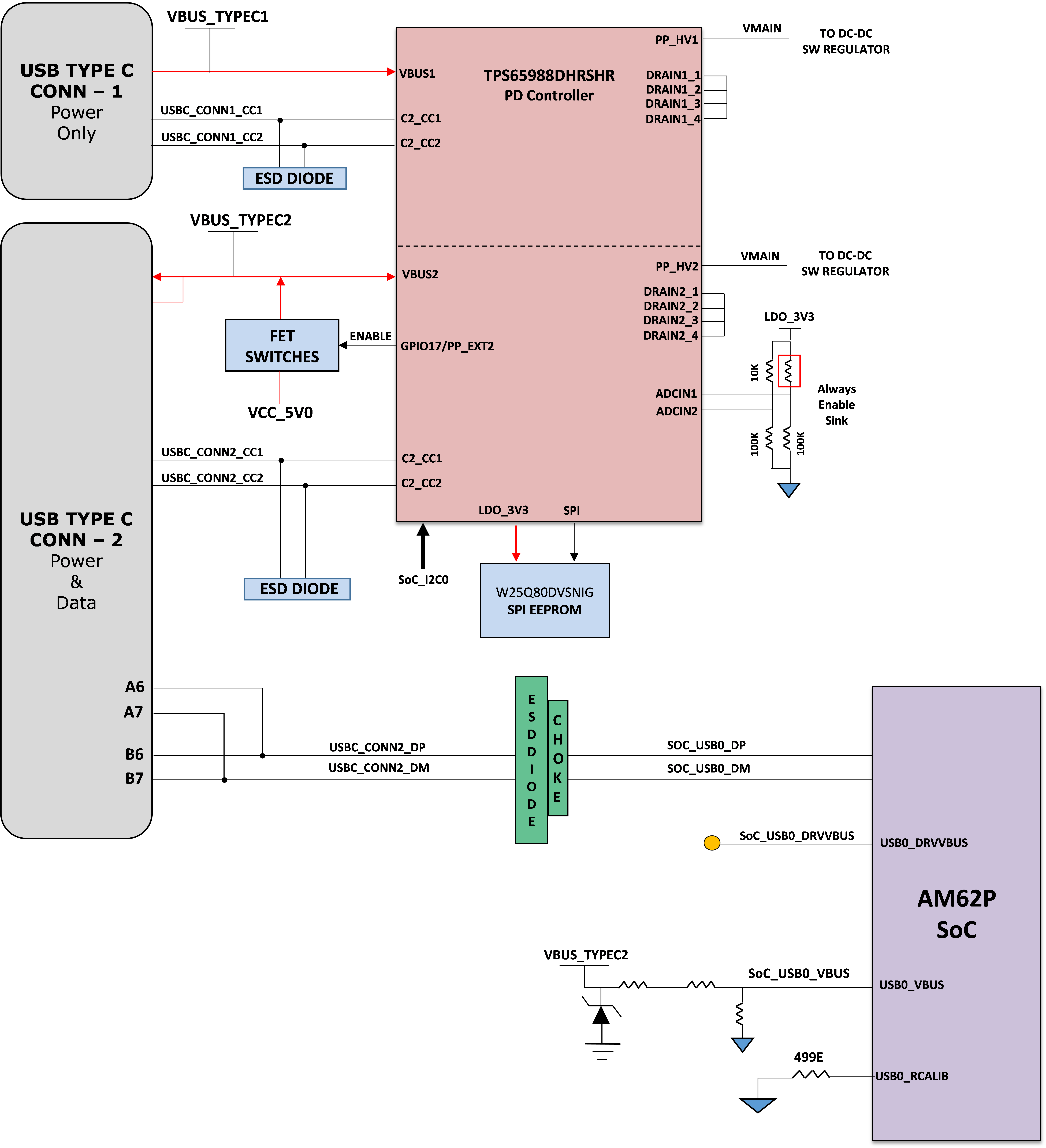
On SK EVM, USB 2.0 Interface is offered through USB Type-C Connector J19 Mfr part# 2012670005 which supports data rate up to 480Mbps. J19 can be used for data communication and as a power connector sourcing supply to the SK EVM. J19 is configured as DRP port using PD controller TPS65988DHRSHR IC. So, J19 can act as either a host or device. The role of the port depends on the type of device getting connected on the connector and the ability to either sink or source. When the port is acting as DFP, DFP can source up to 5 V @ 500 mA.
USB 2.0 data lines DP and DM from J19 are provided with a choke and an ESD protection device. USB0_VBUS to the SOC is provided through a resistor divider network to support (5V-30V) VBUS operation.
A common mode choke of Mfr Part# DLW21SZ900HQ2B is provided on USB data lines for EMI/ EMC reduction. ESD protection devices of part number ESD122DMXR is included to dissipate any ESD strikes on USB2.0 DP/DM signals. An ESD protection device of part number TPD1E01B04DPLT is included on CC signals and TVS2200DRVR IC is included on VBUS rail of Type-C Connector J19 to dissipate ESD strikes.
 Figure 2-16 USB 2.0 Type C
Interface