SPRUJA2 November 2023
- 1
- Description
- Get Started
- Features
- 5
- 1Evaluation Module Overview
-
2Hardware
- 2.1 Additional Images
- 2.2 Key Features
- 2.3 Interface Mapping
- 2.4 Power ON/OFF Procedure
- 2.5 Clocking
- 2.6 Reset
- 2.7 CSI Interface
- 2.8 OLDI Interface
- 2.9 DSI Interface
- 2.10 Audio Codec Interface
- 2.11 HDMI Display Interface
- 2.12 JTAG Interface
- 2.13 Test Automation Header
- 2.14 UART Interface
- 2.15 USB Interface
- 2.16 Memory Interfaces
- 2.17 Ethernet Interface
- 2.18 GPIO Port Expander
- 2.19 GPIO Mapping
- 2.20 Power
- 2.21 EVM User Setup/Configuration
- 2.22 Expansion Headers
- 2.23 Interrupt
- 2.24 I2C Address Mapping
- 3Hardware Design Files
- 4Compliance Information
- 5Additional Information
2.16.2 OSPI Interface
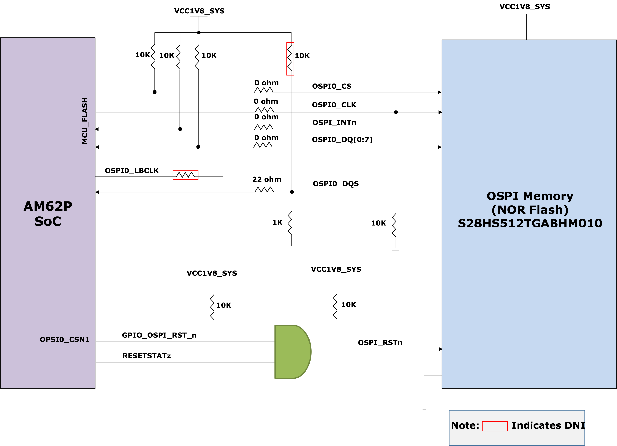
AM62P SK EVM board features a 512Mb OSPI memory device from Cypress Part# S28HS512TGABHM010 connected to the OSPI0 interface of the AM62P SOC. The OSPI memory supports single and double data rates with memory speeds up to 200MBps SDR and 400MBps DDR (200 MHz clock speed).
OSPI & QSPI implementation: 0 ohm resistors are provided for DATA[7:0], DQS, INT# and CLK signals. External pull up resistors are provided on DATA[7:0] to prevent bus floating. The footprint for the OSPI memory also allows the installation of either a QSPI memory or an OSPI memory. The 0 ohm series resistors provided for pins OSPI_DQ[4:7] can be removed if a QSPI Flash is to be mounted.
Reset: The reset for the OSPI flash is connected to a circuit that ANDs the RESETSTATz from the AM62P with the signal GPIO_OSPI_RSTn from the SOC GPIO. A pull-up resistor is provided on GPIO_OSPI_RSTn to set the default active state.
Power: Both VCC and VCCQ pins of the OSPI Flash memory is supplied through an on board 1.8V system power. The OSPI I/O group is powered by the VDDSHV1 domain of SOC sourced from the same 1.8V system power.
 Figure 2-18 OPSI Interface