SPRUJA2 November 2023
- 1
- Description
- Get Started
- Features
- 5
- 1Evaluation Module Overview
-
2Hardware
- 2.1 Additional Images
- 2.2 Key Features
- 2.3 Interface Mapping
- 2.4 Power ON/OFF Procedure
- 2.5 Clocking
- 2.6 Reset
- 2.7 CSI Interface
- 2.8 OLDI Interface
- 2.9 DSI Interface
- 2.10 Audio Codec Interface
- 2.11 HDMI Display Interface
- 2.12 JTAG Interface
- 2.13 Test Automation Header
- 2.14 UART Interface
- 2.15 USB Interface
- 2.16 Memory Interfaces
- 2.17 Ethernet Interface
- 2.18 GPIO Port Expander
- 2.19 GPIO Mapping
- 2.20 Power
- 2.21 EVM User Setup/Configuration
- 2.22 Expansion Headers
- 2.23 Interrupt
- 2.24 I2C Address Mapping
- 3Hardware Design Files
- 4Compliance Information
- 5Additional Information
2.7 CSI Interface
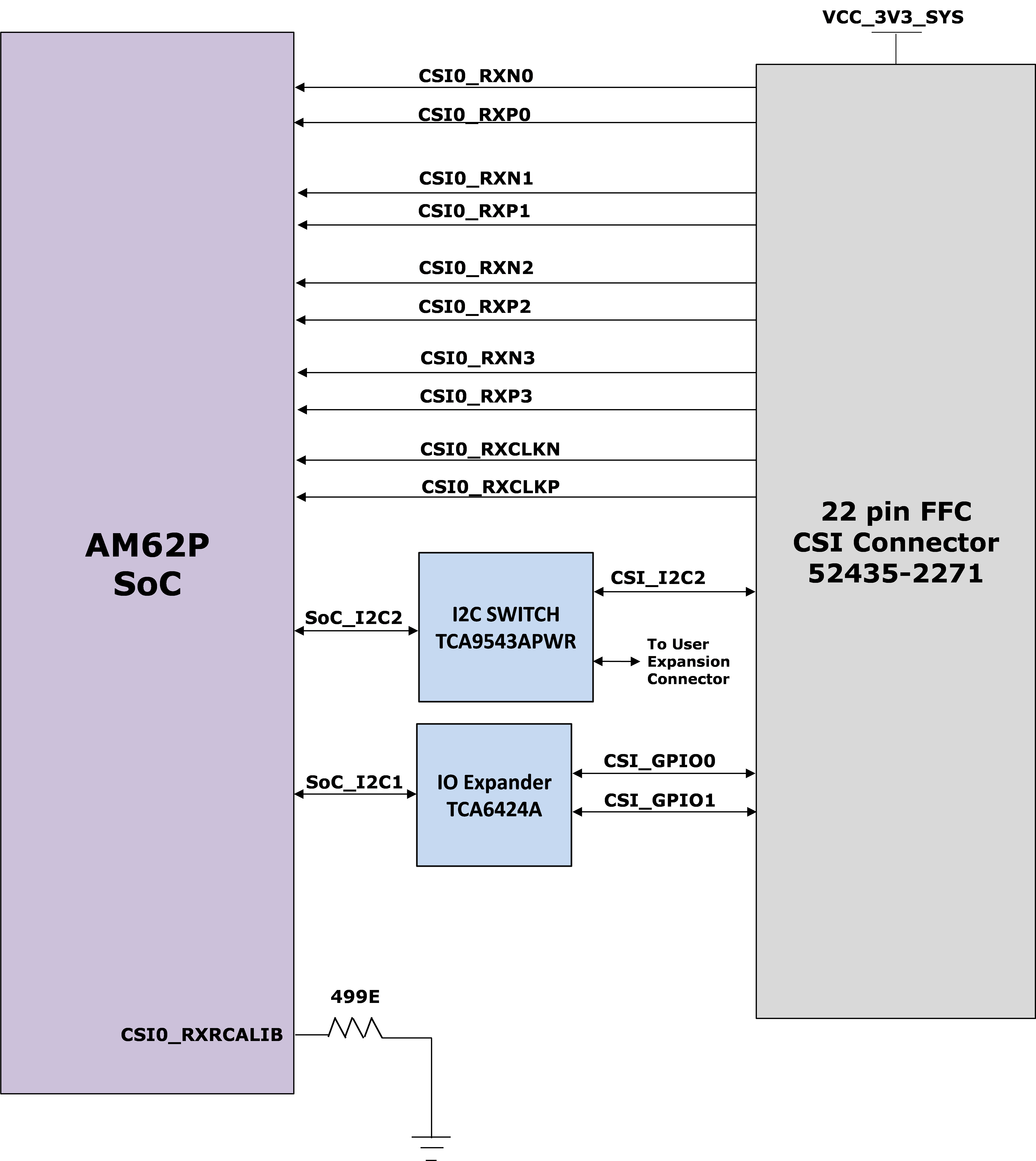
The CSI-2 signals from the AM62P SOC are terminated to a 22 pin FFC connector 52435-2271 to interface with commercially available of the shelf CSI-2 standard Camera Card/Modules. All four CSI RX lanes are pinned out on the SK EVM along with SOC_I2C2 instance and a couple of GPIO’s from the I2C1 controlled GPIO Port Expander.
 Figure 2-7 CSI Interface
Table 2-4 CSI Camera Connector (J6)
Pin-Out
| Pin No | Pin Description |
|---|---|
| 1 | DGND |
| 2 | CSI0_RXN0 |
| 3 | CSI0_RXP0 |
| 4 | DGND |
| 5 | CSI0_RXN1 |
| 6 | CSI0_RXP1 |
| 7 | DGND |
| 8 | CSI0_RXCLKN |
| 9 | CSI0_RXCLKP |
| 10 | DGND |
| 11 | CSI0_RXN2 |
| 12 | CSI0_RXP2 |
| 13 | DGND |
| 14 | CSI0_RXN3 |
| 15 | CSI0_RXP3 |
| 16 | DGND |
| 17 | CSI_GPIO0 |
| 18 | CSI_GPIO1 |
| 19 | DGND |
| 20 | CSI_I2C2_SCL |
| 21 | CSI_I2C2_SDA |
| 22 | VCC_3V3_SYS |