SPRUJE1 July 2024
- 1
- Description
- Get Started
- Features
- 5
- 1Evaluation Module Overview
-
2Hardware
- 2.1 Key Features
- 2.2 Important Usage Notes
- 2.3 Functional Block Diagram
- 2.4 Power ON/OFF Procedures
- 2.5 Peripheral and Major Component Description
- 3Hardware Design Files
- 4Compliance Information
- 5Additional Information
- 6Related Documentation
2.1.2 Power Supply
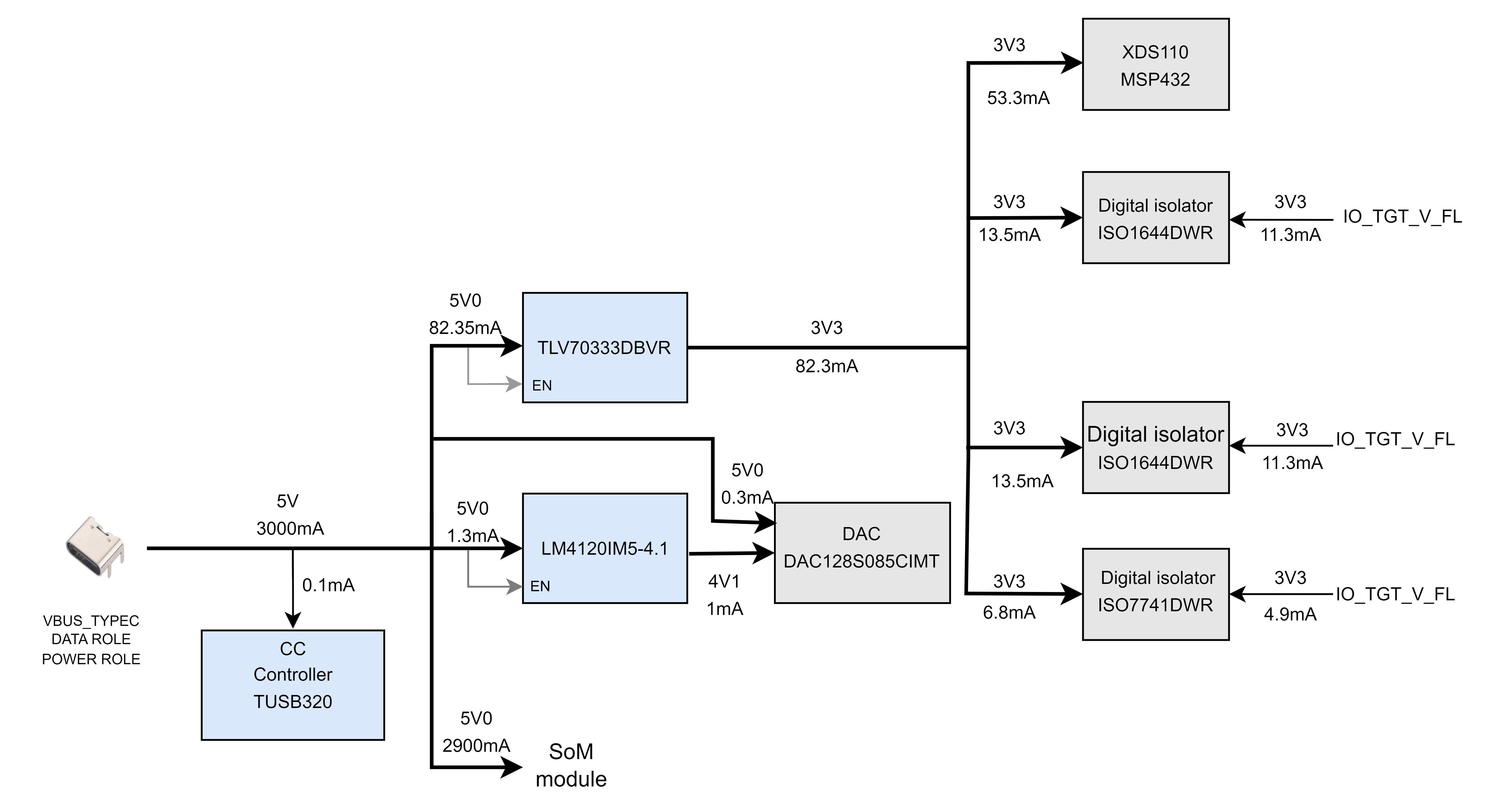
XDS110 board is powered through USB Type-C connector. The same connector is used to negotiate the power role and data role with the source device. The block diagram depicts the power flow of the XDS110 board.
 Figure 2-1 Power Architecture of
XDS110
Figure 2-1 Power Architecture of
XDS110The following sections describe the power distribution network topology that supplies the XDS110 board, supporting components and reference voltages.
The XDS110 board includes a power design based on discrete power supply components. The initial stage of the power supply is VBUS voltage from the USB Type-C connectors J5. USB Type-C CC controller of Mfr. Part# TUSB320LIRWBR is used for negotiation of the required power to the system, role detection, cable orientation.
The DAC reference generator, DAC IC and CC Controller gets power from the 5V input source.
XDS110 board receives the 5V from the type C Connector. TUSB320 CC controller is used to authenticate the 5V/3A source connected. One LDO is used to generate 3V3 from 5V0 for powering the XDS110 MCU MSP432 and digital isolators. Another LDO is used to generate 4V1 from 5V0 for providing reference voltage to the DAC IC. Discrete regulators and LDOs used onboard are:
TUSB320LIRWBR – To authenticate 5V/3A source connected.
LM4120IM5-4.1/NOPB – To generate VREF (4V1) reference voltage for DAC IC.
TLV70333DBVR – To generate VCC_3V3 rail for XDS110 MCU MSP432 and digital isolators.
Additionally, IO_TGT_V_FL is generated by the SOM board for providing 3V3 to digital isolators.