SPRZ255F May 2007 – June 2020 TMS320F28044
3 Device Markings
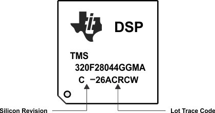
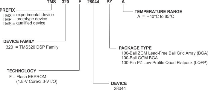
Figure 1 provides an example of the TMS320F28044 device markings and defines each of the markings. The device revision can be determined by the symbols marked on the top of the package as shown in Figure 1. Some prototype devices may have markings different from those illustrated. Figure 2 shows the TMS320F28044 device nomenclature.
 Figure 1. Example of Device Markings
 Table 1. Determining Silicon Revision From Lot Trace Code (F28044)
| SECOND LETTER
IN PREFIX OF LOT TRACE CODE |
SILICON REVISION | REVISION ID
Address: 0x0883 |
F28044 COMMENTS |
|---|---|---|---|
| Blank (no second letter in prefix) | Indicates Revision 0 | 0x0000 | This silicon revision is available as TMX or TMS |
