SPRZ408D June 2014 – June 2021 AM4372 , AM4376 , AM4377 , AM4378 , AM4379
- Trademarks
- 1Introduction
- 2All Errata Listed With Silicon Revision Number
-
3Usage Notes and Known Design Exceptions to Functional Specifications
- 3.1 Usage Notes
- 3.2
Known Design Exceptions to Functional Specifications
- 3.2.1 Advisory List
- Advisory 1
- Advisory 2
- Advisory 3
- Advisory 4
- Advisory 5
- Advisory 6
- Advisory 7
- Advisory 8
- Advisory 9
- Advisory 10
- Advisory 11
- Advisory 12
- Advisory 13
- Advisory 14
- Advisory 15
- Advisory 16
- Advisory 17
- Advisory 19
- Advisory 20
- Advisory 21
- Advisory 22
- Advisory 24
- Advisory 25
- Advisory 26
- Advisory 27
- Advisory 28
- i2223
- i2224
- i912
- i2225
- i2226
- 4Revision History
1.2 Revision Identification
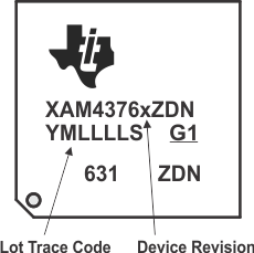
The device revision can be determined by the symbols marked on the top of the package. Figure 1-1 provides an example of the device markings.
 Figure 1-1 Example of Device Revision Codes for the Device Processor
NOTES:
- Non-qualified devices are marked with the letters "X" or "P" at the beginning of the device name, while qualified devices have a "blank" at the beginning of the device name.
- The device shown in this device marking example are two of several valid part numbers for the family of devices.
- The device revision code is the device revision (A, B, and so on).
- YM denotes year and month.
- LLLL denotes Lot Trace Code.
- 631 is a generic family marking ID.
- G1 denotes green, lead-free.
- ZDN is the package designator.
- S denotes Assembly Site Code.
- On some "X" devices, the device speed may not be shown.
Silicon revision is identified by a code marked on the package. The code is of the format AM4376x, where "x" denotes the silicon revision. Table 1-1 lists the information associated with each silicon revision for each device type. For more details on device nomenclature, see the device-specific data manual.
| DEVICE REVISION CODE | SILICON REVISION | COMMENTS |
|---|---|---|
| A | 1.1 | Silicon revision PG1.1 |
| B | 1.2 | Silicon revision PG1.2 |
Each silicon revision uses a specific revision of TI's ARM® Cortex®-A9 processor. The ARM Cortex-A9 processor variant and revision can be read from the Main ID Register. The DEVREV field (bits 31-28) of the Device_ID register located at address 0x44E10600 provides a 4-bit binary value that represents the device revision. The ROM code revision can be read from address 0x3BFFC on silicon revision 1.1 and 0x3FFFC on silicon revision 1.2. The ROM code version consists of two decimal numbers: major and minor. The major number is 0x27, and the minor number counts ROM code version. The ROM code version is coded as hexadecimal readable values; for example, ROM version 27.02 is coded as 0x2702. Table 1-2 shows the ARM Cortex-A9 Variant and Revision, Device Revision, and ROM Code Revision values for each silicon revision of the device.
| SILICON REVISION | ARM CORTEX-A9 VARIANT AND REVISION | DEVICE REVISION | ROM REVISION | PL310 CACHE CONTROLLER VERSION |
|---|---|---|---|---|
| 1.1 | r2p10 | 0001b | 27.01 | r3p2 |
| 1.2 | r2p10 | 0002b | 27.02 | r3p2 |