SPRZ428E November 2014 – September 2024 TDA2E
- 1
- 1Introduction
-
2Silicon Advisories
- Revisions SR 2.1, 2.0, 1.0 - Advisories List
- i202
- i378
- i631
- i694
- i698
- i699
- i709
- i727
- i729
- i734
- i767
- i782
- i783
- i802
- i803
- i807
- i808
- i809
- i810
- i813
- i814
- i815
- i818
- i819
- i820
- i824
- i826
- i829
- i834
- i849
- i856
- i862
- i863
- i867
- i868
- i869
- i870
- i871
- i872
- i874
- i875
- i878
- i879
- i880
- i882
- i883
- i887
- i889
- i890
- i893
- i895
- i896
- i897
- i898
- i899
- i900
- i903
- i904
- i906
- i913
- i916
- i927
- i928
- i929
- i930
- i932
- i933
- i2446
- 3Silicon Limitations
- 4Silicon Cautions
- 5Revision History
i934
VDDA_PCIE to VDDA33V_USB1 Current Path
CRITICALITY
High
DESCRIPTION
An unintended leakage current path between VDDA_PCIE (1.8 V) and VDDA33_USB1 (3.3 V) due to ESD protection diode connection across the signal to I/O supply pads exists. This path can allow current to flow from VDDA_PCIE to VDDA33V_USB1. The current flows whenever the voltage level on VDDA_PCIE exceeds VDDA33V_USB by more than a diode drop during certain power-up and power-down sequences.
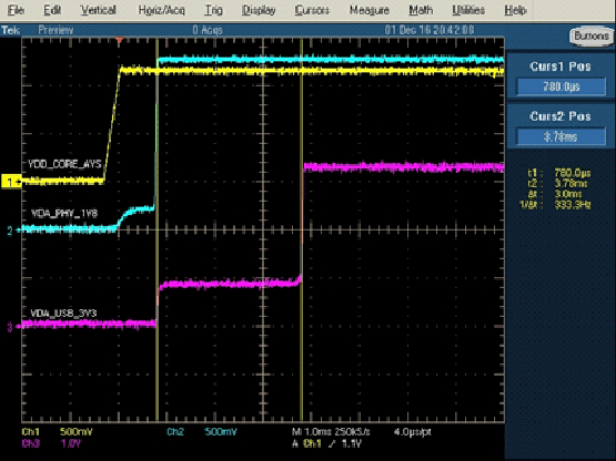
This leakage current causes the un-energized VDDA33V_USB1 to rise to a ~1 V plateau (see Figure 4-3) due to the power resource’s “off impedance” seen between the VDDA33V_USB1 power rail to ground. When the minimum “off impedance” is >= 100 Ω, the SoC leakage current is small and sustainable with no SoC reliability impacts.
 Figure 4-3 Original Power-Up Sequence
Note: Figure 4-3 shows in VDA_PHY_1V8 rail a plateau approximately 250 mV documented in i931, VDD to VDDA_"PHY" Current Path.
GUIDELINES
TI recommended Power Delivery Networks (PDNs) could have multiple different PMIC LDO power resources connected to the VDDA33V_USB1 rail. The LP8733/32 PMICs have a minimum OFF resistance equal to 150 Ω so a PDN using these PMICs would not exceed safe leakage current level and could continue to use the original SoC power sequences. However, the TPS65917/919 PMICs have a minimum OFF resistance equal to 30 Ω and would exceed the safe leakage current limit. As a result, any PDN using TPS65917/919 PMICs must implement the revised power sequencing as shown in DM version D or later. The specific sequence changes are:
- For power-up, energize VDDA_PCIE either concurrently or after VDDA33V_USB1
- For power-down, de-energize VDDA_PCIE either concurrently or before VDDA33V_USB1
The following PMIC OTP IDs have been aligned to the revised power sequencing to avoid any leakage current:
- PDN using a single PIMC: TPS65917/919, OTP IDs = 0x4C/0x4D/0x4E/0x4F
- PDN using dual PMICs: LP8733, OTP ID = 0x2D and LP8732, OTP ID = 0x20
REVISIONS IMPACTED
TDA2Ex (17mm) SR 2.1, 2.0
DRA79x: 2.1, 2.0
TDA2Ex (17mm): 2.1, 2.0
AM570x: 2.1, 2.0
DRA71x: 2.1, 2.0