SPRZ506D October 2022 – December 2024 TMS320F2800132 , TMS320F2800133 , TMS320F2800135 , TMS320F2800137
- 1
- TMS320F28003x Real-Time MCUs Silicon ErrataSilicon Revision 0
- 1Usage Notes and Advisories Matrices
- 2Nomenclature, Package Symbolization, and Revision Identification
-
3Silicon Revision C Usage Notes and Advisories
- 3.1
Silicon Revision C Usage Notes
- 3.1.1 PIE: Spurious Nested Interrupt After Back-to-Back PIEACK Write and Manual CPU Interrupt Mask Clear
- 3.1.2 Caution While Using Nested Interrupts
- 3.1.3 Security: The primary layer of defense is securing the boundary of the chip, which begins with enabling JTAGLOCK and Zero-pin Boot to Flash feature
- 3.2 Silicon Revision C Advisories
- 3.1
Silicon Revision C Usage Notes
- 4Silicon Revision B Usage Notes and Advisories
- 5Silicon Revision A Usage Notes and Advisories
- 6Silicon Revision 0 Usage Notes and Advisories
- 7Documentation Support
- 8Trademarks
- 9Revision History
Advisory
FPU: FPU-to-CPU Register Move Operation Preceded by Any FPU 2p Operation
Revisions Affected
0, A, B, C
Details
This advisory applies when a multicycle (2p) FPU instruction is followed by a FPU-to-CPU register transfer. If the FPU-to-CPU read instruction source register is the same as the 2p instruction destination, then the read may be of the value of the FPU register before the 2p instruction completes. This occurs because the 2p instructions rely on data-forwarding of the result during the E3 phase of the pipeline. If a pipeline stall happens to occur in the E3 phase, the result does not get forwarded in time for the read instruction.
The 2p instructions impacted by this advisory are MPYF32, ADDF32, SUBF32, and MACF32. The destination of the FPU register read must be a CPU register (ACC, P, T, XAR0...XAR7). This advisory does not apply if the register read is a FPU-to-FPU register transfer.
In the example below, the 2p instruction, MPYF32, uses R6H as its destination. The FPU register read, MOV32, uses the same register, R6H, as its source, and a CPU register as the destination. If a stall occurs in the E3 pipeline phase, then MOV32 will read the value of R6H before the MPYF32 instruction completes.
Example of Problem:
   MPYF32 R6H, R5H, R0H  ; 2p FPU instruction that writes to R6H
|| MOV32 *XAR7++, R4H
   F32TOUI16R R3H, R4H   ; delay slot
   ADDF32 R2H, R2H, R0H
|| MOV32 *--SP, R2H      ; alignment cycle
   MOV32 @XAR3, R6H      ; FPU register read of R6H
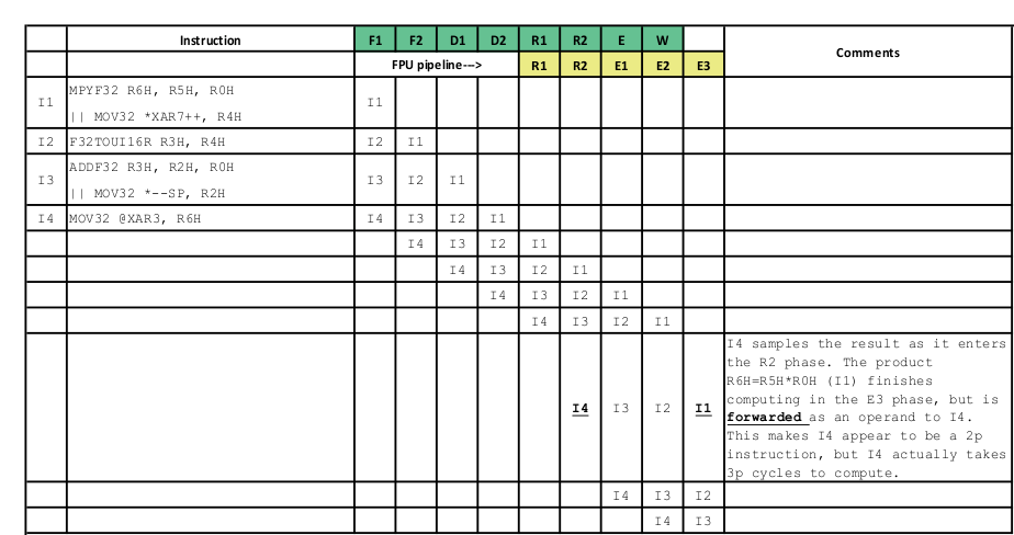
Figure 3-4 shows the pipeline diagram of the issue when there are no stalls in the pipeline.
 Figure 3-4 Pipeline Diagram of the Issue When There are no Stalls in the Pipeline
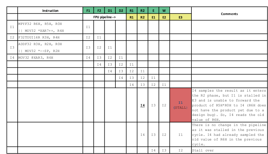
Figure 3-5 shows the pipeline diagram of the issue if there is a stall in the E3 slot of the instruction I1.
 Figure 3-5 Pipeline Diagram of the Issue if There is a Stall in the E3 Slot of the Instruction I1
Workaround
Treat MPYF32, ADDF32, SUBF32, and MACF32 in this scenario as 3p-cycle instructions. Three NOPs or non-conflicting instructions must be placed in the delay slot of the instruction.
The C28x Code Generation Tools v.6.2.0 and later will both generate the correct instruction sequence and detect the error in assembly code. In previous versions, v6.0.5 (for the 6.0.x branch) and v.6.1.2 (for the 6.1.x branch), the compiler will generate the correct instruction sequence but the assembler will not detect the error in assembly code.
Example of Workaround:
   MPYF32 R6H, R5H, R0H
|| MOV32 *XAR7++, R4H     ; 3p FPU instruction that writes to R6H
   F32TOUI16R R3H, R4H    ; delay slot
   ADDF32 R2H, R2H, R0H
|| MOV32 *--SP, R2H       ; delay slot
   NOP                    ; alignment cycle
   MOV32 @XAR3, R6H       ; FPU register read of R6H
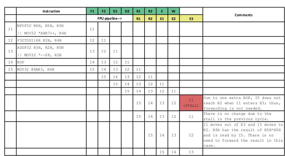
Figure 3-6 shows the pipeline diagram with the workaround in place.
 Figure 3-6 Pipeline Diagram With Workaround in Place