No. 1: FET Losses Calculator
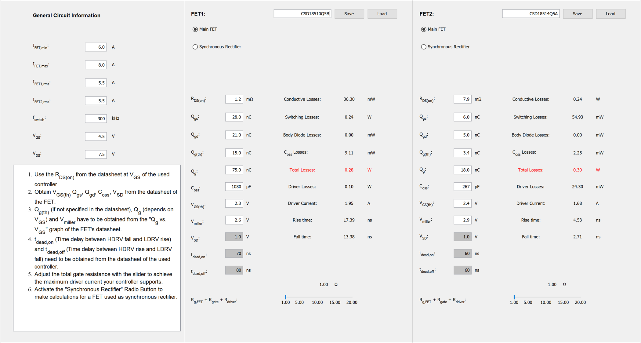
With this tool you can easily compare different FETs that are either operating as a main switch or as a synchronous rectifier. The minimum, maximum and root-mean-square (RMS) current values, FET drain-to-source
voltage and switching frequency will transfer from the chosen topology window. The tool can also help you assess the total metal-oxide semiconductor field-effect transistor (MOSFET) losses of synchronous converters after you’ve chosen
applicable MOSFETs for the main switch and synchronous rectifier. Figure 1 shows the FET losses calculator window.
No. 2: Current-sharing Calculator
When paralleling different kinds of capacitors at the input or output of a power converter, the capacitors experience different amounts of RMS current, depending on their impedance. With Power Stage Designer, you
can estimate the current stress for up to three parallel capacitors based on a first harmonic impedance model.
No. 3: AC/DC Bulk Capacitor Calculator
AC/DC converters typically have a bulk capacitor behind the input rectifier to provide a quasi-constant input voltage to the power stage and power-management controller. Power Stage Designer will suggest the bulk
capacitance based on different input parameters.
No. 4: RC Snubber Calculator for Rectifiers
In power supplies, ringing across rectifiers can be a major issue if you need to pass electromagnetic interference (EMI) testing. There are different methods to deal with this problem, and implementing an RC snubber
network is an easy solution that might keep you from having to redesign your printed circuit board (PCB) layout. Our tool gives you an easy way to determine the starting values for your RC snubber network.
No. 5: RCD Snubber Calculator for Flyback Converters
Due to parasitics such as transformer leakage inductance, flyback converters can experience voltage overshoot and ringing at the switching node. The easiest way to reduce the ringing and to achieve damping of the
overshoot is to implement an RCD snubber circuit in parallel with the primary inductance of your flyback converter. Power Stage Designer can help you choose starting values for the snubber resistor and capacitor.
No. 6: Output-voltage Resistor Divider Calculator
It is now possible to easily calculate the output-voltage feedback divider for your power supply based on the output voltage, reference voltage and high- or low-side resistance, including tolerances.
No. 7: Dynamic Analog Output-voltage Scaling Calculator
For some applications, the output voltage of a power converter needs to be adjustable in a certain output-voltage range. You can accomplish this by feeding a variable analog output voltage with a third resistor to
the output-voltage resistor divider. Power Stage Designer helps you find the values for the resistances needed based on the chosen output-voltage range, maximum adjusting voltage, reference voltage and top feedback resistance.
No. 8: Dynamic Digital Output Voltage Scaling Calculator
It’s also possible to adjust the output voltage of your power supply by paralleling multiple resistor/signal MOSFET combinations with the low-side feedback resistor. By enabling and disabling the MOSFETs with a
microcontroller, it’s as if you’ve “programmed” different output voltages to the power supply. Power Stage Designer will assist you in choosing the resistance values for the feedback circuit.
No. 9: Unit Converter
Power Stage Designer includes a little helper that converts different power-supply parameters, such as gain to factor or imperial to International System of Units, and vice versa.
No. 10: Loop Calculator
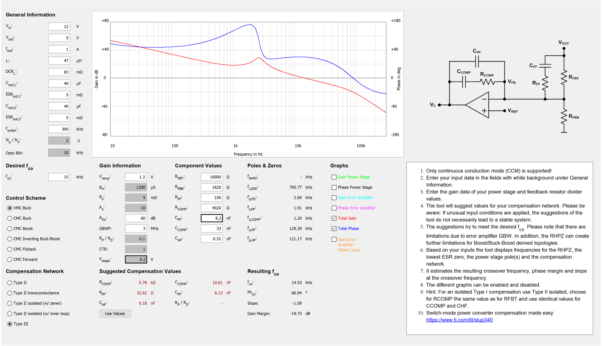
The loop calculator displays Bode plots of the open- and closed-loop transfer functions for the voltage-mode control buck, and five different current-mode control topologies: buck, boost, inverting buck-boost,
forward and flyback. You can use five different compensation networks for closing the loop. Figure 2 shows the Power Stage Designer loop calculator
window.
No. 11: Load-step Calculator
With the load-step calculator, you can determine the required minimum output capacitance for voltage-mode and current-mode-controlled converters to stay within output-voltage regulation requirements. Take care when
using this tool with devices that leverage an internal compensation network, as the degrees of freedom for choosing external components are limited with those kinds of devices.
No. 12: Filter Designer
The filter designer helps you design properly damped differential mode π-filters for power supplies. The tool not only shows the Bode plots of the filter and damping network, but also the graphs of the undamped and
damped filter impedance. With this information, it is possible to simultaneously determine whether the filter provides sufficient signal attenuation and stability with your chosen damping components. The filter designer will provide a very
good starting point, but to meet EMI specifications with a finished PCB, factors such as PCB layout and component parasitics will have a significant impact on the filter’s final performance.
No. 13: New Topologies
- Our Power Stage Designer tool supports a total of 21 topologies, including the four newest ones, the series capacitor buck converter
- Quasi-resonant/frequency-modulated flyback converter
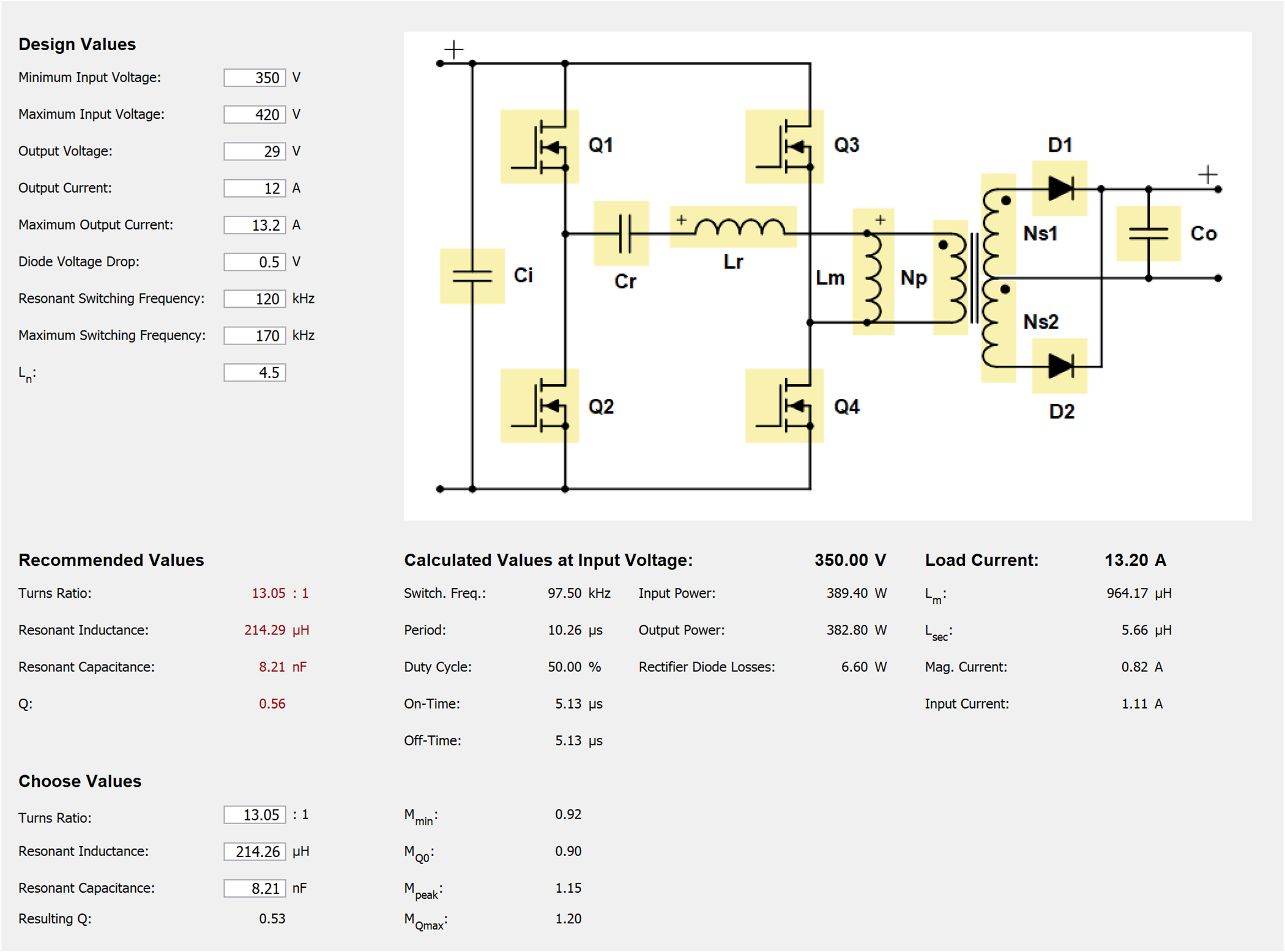
- Inductor-inductor-capacitor (LLC) half-bridge converter
Inductor-inductor-capacitor (LLC) full-bridge converter. See Figure 3.
Power Stage Designer can make your life as a power-supply designer a little bit easier.
For the equations and assumptions behind the new toolbox, see the “Power Stage Designer User’s Guide.”
 Figure 1 FET Losses Calculator Window
 Figure 2 Power Stage Designer Loop Calculator Window
 Figure 3 Topology Window of the LLC Full-bridge Converter