SSZT144 july 2021 CSD15380F3
In part 1 of this series, I reviewed power metal-oxide semiconductor field-effect transistor (MOSFET) data sheets and explained what’s in the data sheet and more importantly, what’s not, while specifically looking at the temperature dependence of some key MOSFET parameters. In part 2, I’ll focus on voltage-dependent leakage currents – the drain-to-source leakage (IDSS) and the gate-to-source leakage (IGSS).
Why leakage currents? There are two fundamental reasons why leakage currents are important when selecting a power MOSFET for your application. First, in electronic systems, there is a green campaign to reduce wasted power, especially when the system is operating in standby mode. And second, in battery-operated systems low leakage helps maximize both battery life for primary cells and the run time between charges for secondary cells.
MOSFET Leakage Currents
 Figure 1 Leakage Current Specifications from the CSD15380F3 Data Sheet
The maximum leakage is specified at one voltage: IDSS at 80% of BVDSS (VGS = 0 V) and IGSS at the absolute maximum VGS (VDS = 0 V). I’m often asked how these parameters vary with voltage, and the answer depends not only on the applied voltage but also on the gate electrostatic discharge (ESD) structure, as detailed in the technical article, “What type of ESD protection does your MOSFET include?” As a refresher, the three types of ESD protection used in TI MOSFETs are none (lowest leakage), single-ended (lowest leakage) and back-to-back (highest leakage).
IGSS Current
 Figure 2 IGSS Vs. vGS With No ESD Protection: 30-v NFET (a); and –20-v PFET (b)
Figure 3 shows IGSS for a 20-V N-channel FET and a –20-V P-channel FET with a single-ended gate ESD protection structure. The leakage current increases exponentially when the gate ESD diode becomes forward-biased. If this is likely to occur in an application, then you must use an external gate resistor to limit the current and prevent damage to the MOSFET.
 Figure 3 IGSS vs. VGS with single-ended ESD protection: 20-V NFET (a); and –20-V PFET (b)
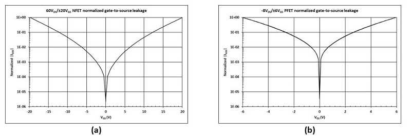
The plots in Figure 4 display IGSS for a 60-V NFET and a –8-V PFET with a back-to-back gate ESD protection structure. These devices display a symmetric leakage characteristic around VGS = 0 V because of the back-to-back gate ESD diodes.
 Figure 4 IGSS vs. VGS with back-to-back ESD protection: 60-V NFET (a); and –8-V PFET (b)
IDSS Current
 Figure 5 IDSS Vs. vDS With No ESD Protection: 30-v NFET (a); and –20-v PFET (b)
Figure 6 shows IDSS for a 20-V N-channel MOSFET and a –20-V P-channel FET, with a single-ended gate ESD protection diode.
 Figure 6 IDSS Vs. vDS With Single-ended ESD Protection: 20-v NFET (a); and –20-v PFET (b)
The plots in Figure 7 display IDSS for a 12-V N-channel MOSFET and a –20-V P-channel MOSFET with the back-to-back gate ESD protection structure.
 Figure 7 IDSS Vs. vDS With Back-to-back ESD Protection: 12-v NFET (a); and –20-v PFET (b)
Conclusion
Additional Resources
- Visit the TI MOSFET support and training center.
- Check out these technical articles