-
How to Choose a Power Supply for an Automotive Camera Module
How to Choose a Power Supply for an Automotive Camera Module
Matthew Sauceda
As automotive camera technology advances with higher resolutions, dynamic ranges and frame rates, power-supply architectures need tailoring to the specific use-case requirements. In this article, I’ll review three strategies you can use to power your automotive camera module:
- Fully discrete
- Fully integrated
- Partially integrated
The focus in this article is on small-form-factor camera modules that don’t include any data processing, and output raw video data to a separate electronic control unit. These modules are often found in surround-view, driver-monitoring and mirror-replacement systems and receive a pre-regulated supply voltage over the same coaxial cable used for video data output.
How much power do you need for a camera module?
The first step when designing the power portion of a camera module is a brief calculation of the power budget for each rail. This, along with the voltage provided over power-over-coax (PoC), is important in selecting the power strategy.
A camera sensor and external circuitry require a current draw that may vary widely across different sensors and any additional external devices. Usually, the lower imager rails (1.2 V and 1.8 V in Figure 1) require the most current, while the largest supply voltage (2.9 V for the imager) requires the least. Because the 2.9-V rail pertains to the analog supply of the imager – and ultimately, its performance with regard to image quality – selecting a supply will require careful consideration, as the rail requires a clean supply with minimal noise. The included FPD-Link device, along with any form of supervisors or sequencers, will also pull from this power budget.
 Figure 1 Calculating the power budget
for each rail
Figure 1 Calculating the power budget
for each railOne might suggest using a low-dropout regulator (LDO) for every supply considering its excellent noise performance. However, that is not feasible when designing with a limited power budget. Additionally, increasing current will stress connectors and cables and increase self heating of the camera, which may worsen performance.
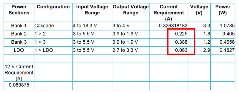
As shown in the example calculation in Table 1, the current requirements for camera modules are generally determined by the sensor and FPD-Link device included in the system. In this example, the imager rails are 1.2 V, 1.8 V and 2.9 V. The FPD-Link device shares the same 1.8-V rail. The required currents for normal operation are highlighted in red.
 Figure 2 Table 1: An example calculation with imager rails at 1.2 V, 1.8 V and 2.9
V
Figure 2 Table 1: An example calculation with imager rails at 1.2 V, 1.8 V and 2.9
VIn this example, the PoC supply over the coaxial cable is first stepped down to 3.3 V, which then supplies the rest of the system on the camera module. The 2.9-V sensor analog rail is tied directly to an LDO output, while the other supplies are tied to a step-down (buck) converter. The 1.8-V rail supplies both the DS90UB953-Q1 supply, and the interface supply of the imager. Since the current consumed by the DS90UB953-Q1 serializer is predominantly greater than the imager interface supply, the 1.8-V current provided to the imager can be considered as negligible. The imager 2.9-V analog rail requires 63 mA, the DS90UB953-Q1 serializer 1.8-V rail requires 225 mA and the imager digital 1.2-V rail requires 388 mA. Assuming 100% efficiency to simplify calculations with the previous values, it is calculated that the 3.3-V supply will require 327 mA to successfully power the 1.2-V, 1.8-V, and 2.9-V rails.
Because the input and output voltages, output current requirements, and total wattage consumption are known, the input current can be calculated with:
(PoC Voltage)*(Current Required) = 3.3-v * 327 mA
For a PoC Voltage of 12-v, the ECU Would Source 90 mA.
In some situations, the PoC voltage is fixed from the ECU, therefore it’s important to understand if the chosen PoC cable and network is adequate in supplying the required current for the power goal. For a 2-W camera module requirement, a fixed 5-V supply would source 400 mA, while a 12-V supply would source 166 mA.
For larger PoC cable lengths, a large PoC voltage should be chosen to ensure minimal IR drop across the cable. PoC current will create a voltage drop across the cabling, ferrite beads, inductors, and any series resistance and will reduce voltage headroom impacting camera module regulator performance. In the case that the PoC voltage value is left to the designer, cable specifications generally dictate the amount of current that the network can provide, which will drive the voltage requirement of the network.
Three power architectures for automotive camera modules
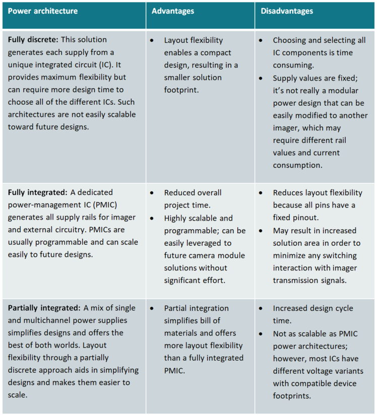
Table 2 compares the advantages and disadvantages of the three different power architectures.
 Figure 3 Table 2: Comparing camera
module power architectures
 Supply considerations
When designing for automotive applications, there are a few considerations that will limit your power design choices. Important system-level specifications include:
- Minimizing the total solution size to meet the small form factor of automotive camera module enclosures. Such enclosures are typically around 20 mm by 20 mm in area and usually fit within an M12 barrel plastic enclosure.
- Avoiding interference with the AM radio band. All switching power supplies need to be outside the AM radio band of 540 kHz to 1,700 kHz.
- Avoiding lower switching frequencies because they require large inductors. Instead, choose:
- High-frequency switchers (>2 MHz).
- Devices that are Automotive Electronics Council-Q100 rated.
- Electronics that need added protection such as a short-to-battery can design with wide Vin regulators.
Printed circuit board constraints
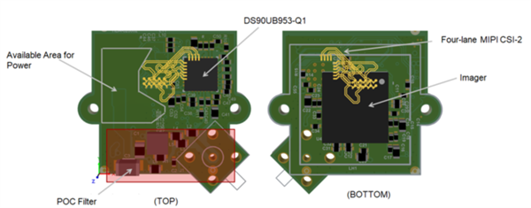
The imager in Figure 4 uses a Mobile Industry Processor Interface (MIPI) Camera Serial Interface (CSI-2), with nets highlighted to display the controlled impedance traces that connect the FPD-Link device to the imager. CSI-2 nets of the imager are brought out through vias and routed mid-layer (highlighted).
The via array poses some limitations to a smaller form factor, as they limit the area of where the power devices can be placed. To minimize coupling, especially around switch-mode power supplies or signal nets, it’s important that CSI-2 nets are properly distanced, shielded and have no overlap from other nets on adjacent layers.
 Figure 4 Example layout of the DS90UB953-Q1 with an imager
Choose your power architecture
The right power architecture will vary based on your design requirements. These reference designs will help you see the specifications in greater detail and make your design simpler when you’re ready to get started:
- Fully discrete: Automotive 2-MP Camera Module Reference Design with MIPI CSI-2 Video Interface, FPD-Link III and POC.
- Fully integrated: Automotive 2-MP Camera Module Reference Design with MIPI CSI-2 Interface, PMIC, FPD-Link III and POC.
- Partially integrated, part 1: Automotive 2-MP Camera Module Reference Design with MIPI CSI-2 Video Interface, FPD-Link III and POC and part 2: Automotive 2.6-MP Camera Module Reference Design with POL PMIC, FPD-Link III, Supervisor and POC.
IMPORTANT NOTICE AND DISCLAIMER
TI PROVIDES TECHNICAL AND RELIABILITY DATA (INCLUDING DATASHEETS), DESIGN RESOURCES (INCLUDING REFERENCE DESIGNS), APPLICATION OR OTHER DESIGN ADVICE, WEB TOOLS, SAFETY INFORMATION, AND OTHER RESOURCES “AS IS” AND WITH ALL FAULTS, AND DISCLAIMS ALL WARRANTIES, EXPRESS AND IMPLIED, INCLUDING WITHOUT LIMITATION ANY IMPLIED WARRANTIES OF MERCHANTABILITY, FITNESS FOR A PARTICULAR PURPOSE OR NON-INFRINGEMENT OF THIRD PARTY INTELLECTUAL PROPERTY RIGHTS.
These resources are intended for skilled developers designing with TI products. You are solely responsible for (1) selecting the appropriate TI products for your application, (2) designing, validating and testing your application, and (3) ensuring your application meets applicable standards, and any other safety, security, or other requirements. These resources are subject to change without notice. TI grants you permission to use these resources only for development of an application that uses the TI products described in the resource. Other reproduction and display of these resources is prohibited. No license is granted to any other TI intellectual property right or to any third party intellectual property right. TI disclaims responsibility for, and you will fully indemnify TI and its representatives against, any claims, damages, costs, losses, and liabilities arising out of your use of these resources.
TI’s products are provided subject to TI’s Terms of Sale (www.ti.com/legal/termsofsale.html) or other applicable terms available either on ti.com or provided in conjunction with such TI products. TI’s provision of these resources does not expand or otherwise alter TI’s applicable warranties or warranty disclaimers for TI products.
Mailing Address: Texas Instruments, Post Office Box 655303, Dallas, Texas 75265
Copyright © 2023, Texas Instruments Incorporated