SSZT436 July 2019 TPS62864 , TPS62866
The miniaturization trend in consumer electronics has taken hold for good. Consumers are demanding smaller electronics with better features: more flash capacity in solid-state drives, faster smartphones, more integrated communication modules, etc. To achieve this, engineers must look for increasingly power dense solutions. One challenge associated with achieving a high-power-density solution is finding small DC/DC converters with compact external components. When it comes to size, DC/DC converters in wafer chip-scale packages (WCSPs) are smaller than standard quad flat no-lead (QFN) or small-outline transistor (SOT) packages. WCSPs have also lower height than QFN or SOT packages, which can help engineers design not only smaller equipment but also one with a lower profile.
The Trouble with Logic Signal Pins
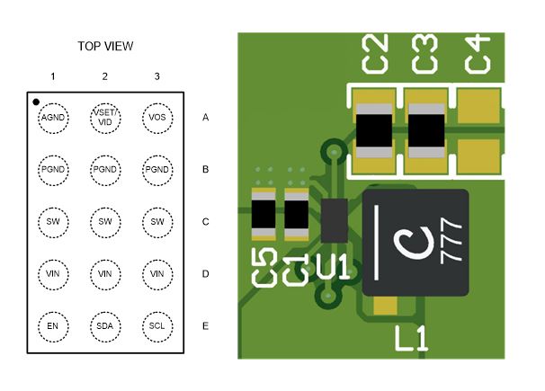
To address this problem, engineers should consider the pinout assignment when choosing the right buck converters in WSPC for their solutions. TI’s TPS62866 is a 6-A synchronous step-down converter which measures only 1.05x1.75x0.5-mm in WCSP. For the same current level buck converters in QFN, the typical package size is 3x3x1-mm. Figure 1 shows the pinout assignment and typical PCB layout of the TPS62866.
 Figure 1 Pinout of the TPS62866 With a Typical PCB Layout
The absence of logic pins in the middle of the integrated circuit means that engineers don’t need special vias for PCB routing, even though the pin pitch is 0.35 mm. Such assignment makes it also possible to place all signal traces around the device for direct routing, further saving board space and allowing engineers to shrink the overall power supply solution, leaving more room for the features that consumers crave.
A reasonable pinout assignment is an important feature for DC/DC converters in WCSP packages. The TPS62866 provides a good pinout assignment and implements many features including I2C interface in a 1.05x1.75x0.5-mm, 0.35-mm pitch WCSP.
Additional Resources
- Read this application note to learn more about the die size BGA (DSBGA) wafer level chip scale package (WLCSP).
- Explore different methods of output-voltage adjustment for DC/DC converters.