Achieving the Programmable Power Supply Function in USB PD Applications
As smartphones continue to get smarter and larger, battery capacitance is also increasing. Being able to quickly charge a battery is a crucial aspect to consider in power delivery. The rise in popularity of USB Type-C™ with USB Power Delivery (PD) and its programmable power supply (PPS) function lowers charge time by maximizing efficiency in the power adapter and minimizing charging losses on the phone end. PPS allows the adapter to have a variable output voltage by communicating with the device being charged, optimizing charging conditions.
The isolated flyback power-supply topology is popular in mobile phone adapters because of its low cost and minimal components. Figure 1 shows the flyback system block diagram. Generally, the main output voltage feedback circuit includes an opto-coupler and a shunt regulator such as TI’s LMV431.
 Figure 1 An Adapter Power Stage
For a common USB PD adapter product, the output voltage range is 3-20V. An easy method for powering the shunt reference is directly from the output. Selecting LMV431 low-voltage/wide adjustable range (1.24V/30V) shunt regulator will help maintain compatibility with a 3.0V lower output voltage. The common fixed output of a mobile adapter is 5V at 1A and only requires two feedback resistors. However, to create a PPS system, the TPL0102-100 enables a variable output.
The TPL0102 has two linear-taper digital potentiometers (DPOTs) with 256 wiper positions and an end-to end resistance of 100kΩ. The TPL0102-100 features two 256-tap digital potentiometers, an I2C interface to communicate with the phone’s microcontroller (MCU) and nonvolatile memory that can store the wiper position. Figure 2 shows the TPL0102-100 in voltage divider mode with a unity gain operational amplifier buffer to create an 8-bit digital-to-analog converter. The analog output voltage of the circuit is determined by the wiper setting, programmed through the I2C bus. A unity gain buffer operational amplifier buffers the high-impedance output of the TPL0102-100; otherwise the loading placed on the output of the voltage divider will affect the output voltage. For PPS, you will need to turn on Q1, a small signal N-channel metal-oxide semiconductor field-effect transistor (MOSFET). It is important to remember that the default value of the TPL0102-100 is 8E for the wiper; therefore the MCU needs to initiate the value of the TPL0102 wiper such that when PPS is turned on, the output voltage value is still 5V.
 Figure 2 Achieving PPS on the Adapter
Side
Figure 2 Achieving PPS on the Adapter
SideDesign Process
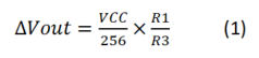
As previously noted, a common mobile adapter output is 5V at 1A. To begin designing a PPS system, you’ll have to calculate R1 and R2 to the default 5V output. Once R1 and R2 have their values locked in, you can then calculate R3 to have the minimum 20mV steps required in PPS systems.
Equation 2 then calculates the output range of Vout:
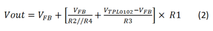
VTPL0102’s range is from 0V to VCC. VFB is the selected shunt regulator’s reference voltage. In the case of the LMV431, the VFB is 1.24V. VCC is the operational amplifier’s power supply and Vout is the adapter output voltage.
USB PD PPS is becoming more and more popular. Configuring the traditional adapter to the PPS function with minimum components and low cost is a challenge, but with some additional circuitry, mobile adapters can easily achieve the PPS function in the latest USB PD technology.
IMPORTANT NOTICE AND DISCLAIMER
TI PROVIDES TECHNICAL AND RELIABILITY DATA (INCLUDING DATASHEETS), DESIGN RESOURCES (INCLUDING REFERENCE DESIGNS), APPLICATION OR OTHER DESIGN ADVICE, WEB TOOLS, SAFETY INFORMATION, AND OTHER RESOURCES “AS IS” AND WITH ALL FAULTS, AND DISCLAIMS ALL WARRANTIES, EXPRESS AND IMPLIED, INCLUDING WITHOUT LIMITATION ANY IMPLIED WARRANTIES OF MERCHANTABILITY, FITNESS FOR A PARTICULAR PURPOSE OR NON-INFRINGEMENT OF THIRD PARTY INTELLECTUAL PROPERTY RIGHTS.
These resources are intended for skilled developers designing with TI products. You are solely responsible for (1) selecting the appropriate TI products for your application, (2) designing, validating and testing your application, and (3) ensuring your application meets applicable standards, and any other safety, security, or other requirements. These resources are subject to change without notice. TI grants you permission to use these resources only for development of an application that uses the TI products described in the resource. Other reproduction and display of these resources is prohibited. No license is granted to any other TI intellectual property right or to any third party intellectual property right. TI disclaims responsibility for, and you will fully indemnify TI and its representatives against, any claims, damages, costs, losses, and liabilities arising out of your use of these resources.
TI’s products are provided subject to TI’s Terms of Sale (www.ti.com/legal/termsofsale.html) or other applicable terms available either on ti.com or provided in conjunction with such TI products. TI’s provision of these resources does not expand or otherwise alter TI’s applicable warranties or warranty disclaimers for TI products.
Mailing Address: Texas Instruments, Post Office Box 655303, Dallas, Texas 75265
Copyright © 2023, Texas Instruments Incorporated