SSZT771 march 2018 TPIC74100-Q1 , TPS55160-Q1 , TPS55162-Q1 , TPS55165-Q1
Automotive body electronics and gateway modules must operate without interruption, regardless of variations in the car battery. A car’s battery voltage can drop down to below 3V during cold crank and may surge as high as 40V during load dump, thus necessitating a DC/DC power supply to both step up and step down and maintain a regulated operating voltage from 5V to 12V.
In addition, DC/DC power supplies should have a small solution size in order to save space, operate with low quiescent current for minimal drainage of the car battery, and be capable of 2MHz switching to avoid electromagnetic interference (EMI) in the AM band. In this blog post, I will compare typical conventional DC/DC power-supply solutions and examine the advantages offered by integrated wide input voltage (VIN) buck-boost converters.
Conventional Solutions
Figure 1 and Figure 2 offer straightforward and quick solutions by cascading two power stages, using one buck and one boost. You can save development time when both the buck and boost stages are existing designs. A main drawback is the low efficiency caused by the two conversion stages. For instance, even if each stage can achieve 90% efficiency, the overall efficiency is the product of the two, yielding 81%. Another drawback is the relatively higher bill-of-materials (BOM) cost and larger solution size – owing to the use of two power inductors, two controllers and more peripheral components, which may duplicate some functions of the two controllers.
Figure 3 shows a single-ended primary-inductor converter (SEPIC) converter, achieving the power conversion in a single stage. However, it still requires two inductors. Although you can use coupled inductors to replace two separate ones, the former undoubtedly costs more than the latter. The AC coupling capacitor that the SEPIC requires also adds to the BOM cost.
Figure 4 shows a buck-boost converter. It is a single-stage converter and only needs one power inductor. The non-synchronous rectifier reduces overall efficiency.
 Figure 1 Conventional Architecture No. 1: Pre-boost Followed by Buck
 Figure 2 Conventional Architecture No. 2: Buck Followed by Post-boost
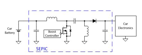 Figure 3 Conventional Architecture No. 3: SEPIC
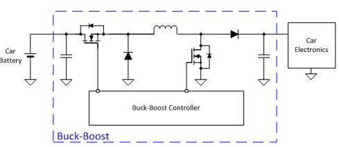 Figure 4 Conventional Architecture No. 4: Buck-boost
Using the synchronous rectifiers as shown in Figure 5 improves the efficiency, but four external MOSFETs raises the BOM cost. There are also challenges associated with difficulty in the printed circuit board (PCB) layout and the routing of power components for optimal performance.
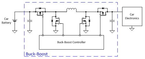 Figure 5 Synchronous Buck-boost
Highly Integrated Wide vIN Buck-boost Converters
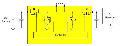 Figure 6 Integrated Single-stage Single-inductor Solution: Buck-boost Converter
An Application Example
Figure 8 shows the circuit’s performance under cold cranking. You can see that the output voltage is solidly regulated at 5V even during transient conditions.
 Figure 7 A Complete Solution with the TPS55165-Q1 for a 5V/1A Application
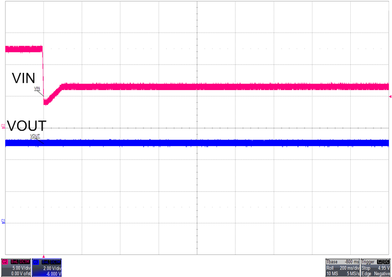 Figure 8 Battery Voltage Cranking Response (Conditions: IOUT = 0.5A, vIN Transient: 12V to 4V)
Conclusion
Additional Resources
- Watch a video that demonstrates the start/stop functionality of a vehicle and presents the various power tree topologies that can handle the start/stop conditions.
- See how cold-crank functions of a vehicle impact the power supply during harsh operating conditions in this video.
- Check out the product pages for the TPS55160-Q1, TPS55162-Q1 and TPS55165-Q1, where you can also find the links to the data sheets, EVMs, Pspice models and the WEBENCH® online simulator.