How to Select a MOSFET – Switch Mode Power Supply
Perhaps the most common use for high-performance power MOSFETs in the current marketplace also presents the greatest challenge in selecting the most appropriate FET. Never are the trade-offs between performance, price and size more muddled than in the case with MOSFETs used in switch-mode power supplies (SMPSs).
Traversing an exhaustive list of SMPS topologies, both isolated and nonisolated, and listing the most important considerations for each would probably take a novel – and an applications expert with far more technical knowledge than a simple marketing engineer like me. But I do hope that in the proceeding paragraphs of this blog, I can offer at least a few tips and traps to avoid.
Most SMPS applications in today’s market operate at relatively high frequencies, from 100kHz all the way into the megahertz range. That means that unlike low-frequency applications like motor control, FET selection is not just about resistance and conduction losses. The higher the frequency, the greater the switching losses, which means that the best-performing or highest-efficiency FET is the one that best optimizes the trade-offs between low gate (and other) charges and low on-resistance, RDS(on).
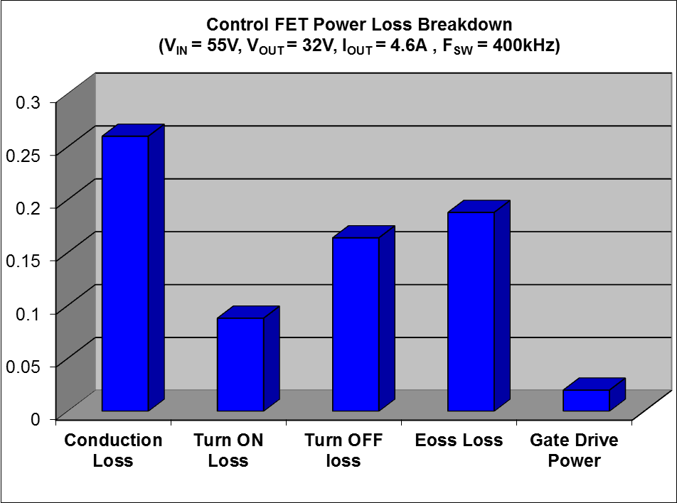
Speaking of charges, it’s not all necessarily about gate charge either. The gate charge, QG, dictates the FET’s ability to turn on and off quickly, an important consideration for hard-switching applications where the faster the turn off, the less duration of voltage/current overlap. That is why the classic MOSFET silicon figure of merit (FOM) is RDS(ON) * QG, with the lowest value indicative of the best performance. But other switching parameters can be as – or more – important depending on the application. During high-side switching, stored energy losses, EOSS, dictated by output capacitance, COSS, can have a large impact on overall system efficiency (see Figure 1).
 Figure 1 Power-loss Breakdown of the
Control FET in a Buck Converter Application
Figure 1 Power-loss Breakdown of the
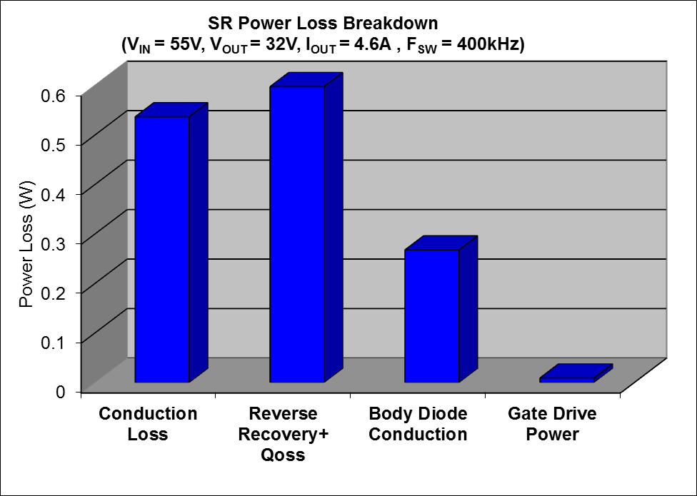
Control FET in a Buck Converter ApplicationIn order to achieve the higher efficiencies that contemporary power-supply energy standards demand, MOSFETs are replacing the sockets historically maintained by diodes to serve as synchronous rectifier switches (see Figure 2). For synchronous rectifier FETs, reverse-recovery losses dictated by the reverse-recovery charge of the MOSFET’s body diode, QRR, can often be the biggest contributors to power loss next to those conduction losses. For such applications, a more relevant FOM is RDS(ON) * (1/2 QOSS + QRR). Figure 3 shows a power-loss breakdown for an 80V MOSFET used in a typical synchronous rectification application.
 Figure 2 In Many Applications, a
Low-resistance MOSFET Replaces the Rectifying Diode to Improve
Efficiency
 Figure 3 Power-loss Breakdown of a
Synchronous Rectifier
Figure 3 Power-loss Breakdown of a
Synchronous RectifierWithin a given FET technology for which respective FOMs are relatively equal, the lower the resistance, the higher the gate charge. Therefore, the most efficient solution is one that optimizes the respective contributions of both conduction and switching losses.
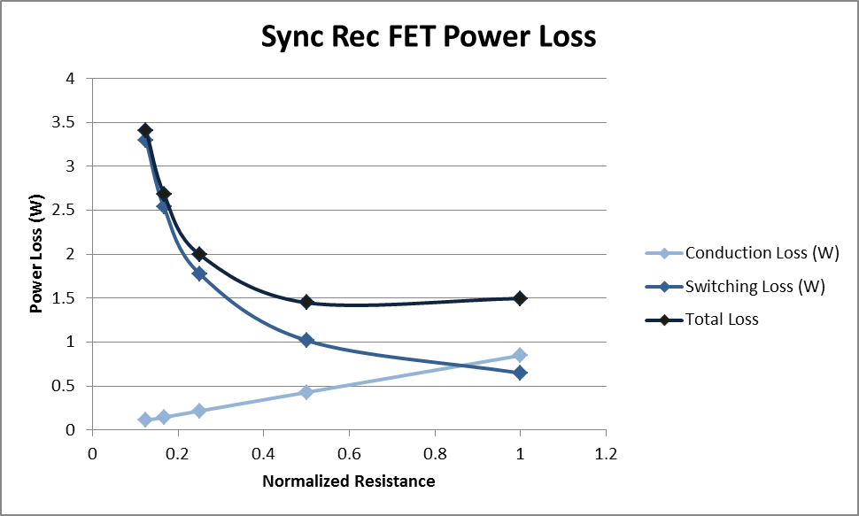
Consider a recent example in which a TI customer wanted a recommendation for a synchronous rectifier FET (for a given set of input conditions and specific output current). Figure 4 shows the respective conduction and switching losses for five different resistance FET options available. Note that the fourth and fifth options yielded very similar total power losses under these conditions, where the curve is more or less flat between the two. However, the fifth option is 2x the resistance of the fourth. Within a FET technology, resistance is inversely proportional to die size, so you can assume (correctly) that the fifth option is a significantly more cost-effective solution.
 Figure 4 Power Loss of Five Different
MOSFET Options – Note That the Fourth and Fifth Options Have Very Similar Total
Losses, Although Different Conduction and Switching Losses
Figure 4 Power Loss of Five Different
MOSFET Options – Note That the Fourth and Fifth Options Have Very Similar Total
Losses, Although Different Conduction and Switching LossesA few last points to consider:
- It is not uncommon for an SMPS application to require a solution that parallels multiple FETs, particularly for synchronous rectifiers. Remember that differences in resistance between FET options will shrink by a factor proportional to the number of FETs you are paralleling. But at the same time, differences in charges will multiply by the same factor, such that at a certain number of FETs, the switching losses will work to decrease overall system efficiency.
- Package selection matters as well. While older packages like transistor outline TO-220 and D2PAK can fit massive silicon die inside and dissipate large amounts of power (particularly through hole devices mounted to a large heat sink), they also have significantly higher package resistance than quad-flat no lead (QFN) devices. Also, at high frequencies, parasitic elements like the MOSFET’s source tab inductance begin to play a greater role and can have devastating impacts on switch-node ringing and overall system efficiency. Therefore, QFN packages (like TI’s SON5x6 or SON3x3) can achieve higher power density than their TO counterparts, and are almost always better suited for driving higher frequencies in the range of several hundred to a thousand kilohertz. That is why QFN packages like TI’s small outline no lead (SON) 5mm by 6mm or SON 3mm by 3mm can achieve higher power density than their TO counterparts, and are almost always better suited for driving higher frequencies in the range of several hundred to a thousand kilohertz.
- You can discern some critical SMPS parameters, like RDS(on) and QG, straight from the MOSFET’s data sheet. Other parameters on the data sheet, like QRR and QOSS, are much more unreliable. Therefore, it is better to obtain an on-board, apples-to-apples measurement in order to get a fair comparison across different FET vendors.
If this post has only served to further muddy the waters and make the FET selection for SMPS applications appear more complicated than you previously thought, that was by design. FET selection is no trivial task and should not be treated as such. However, in the next installment of this series, I will discuss one extremely useful tool that TI has developed to make the selection of MOSFETs for one particular SMPS application – synchronous buck converters – as simple as plugging in a few parameters and analyzing the performance vs. cost trade-offs. Questions? Please feel free to leave a comment below.
IMPORTANT NOTICE AND DISCLAIMER
TI PROVIDES TECHNICAL AND RELIABILITY DATA (INCLUDING DATASHEETS), DESIGN RESOURCES (INCLUDING REFERENCE DESIGNS), APPLICATION OR OTHER DESIGN ADVICE, WEB TOOLS, SAFETY INFORMATION, AND OTHER RESOURCES “AS IS” AND WITH ALL FAULTS, AND DISCLAIMS ALL WARRANTIES, EXPRESS AND IMPLIED, INCLUDING WITHOUT LIMITATION ANY IMPLIED WARRANTIES OF MERCHANTABILITY, FITNESS FOR A PARTICULAR PURPOSE OR NON-INFRINGEMENT OF THIRD PARTY INTELLECTUAL PROPERTY RIGHTS.
These resources are intended for skilled developers designing with TI products. You are solely responsible for (1) selecting the appropriate TI products for your application, (2) designing, validating and testing your application, and (3) ensuring your application meets applicable standards, and any other safety, security, or other requirements. These resources are subject to change without notice. TI grants you permission to use these resources only for development of an application that uses the TI products described in the resource. Other reproduction and display of these resources is prohibited. No license is granted to any other TI intellectual property right or to any third party intellectual property right. TI disclaims responsibility for, and you will fully indemnify TI and its representatives against, any claims, damages, costs, losses, and liabilities arising out of your use of these resources.
TI’s products are provided subject to TI’s Terms of Sale (www.ti.com/legal/termsofsale.html) or other applicable terms available either on ti.com or provided in conjunction with such TI products. TI’s provision of these resources does not expand or otherwise alter TI’s applicable warranties or warranty disclaimers for TI products.
Mailing Address: Texas Instruments, Post Office Box 655303, Dallas, Texas 75265
Copyright © 2023, Texas Instruments Incorporated