SSZT844 December 2017 SN65HVD888 , TLV61046A , TPS61046
RS-485 is a standard defining the electrical characteristics of drivers and receivers for use in serial communication systems. It defines not only a single device-to-device interface, but also a communications bus that can form simple networks of multiple devices.
RS-485 runs on twisted-pair cable, and the voltage differential of the two lines defines the logic, as shown in Figure 1. Because of its simplicity, low cost and good noise immunity, RS-485 is widely used in factory automation, building automation and metering applications.
 Figure 1 RS-485 Network
Structure
Figure 1 RS-485 Network
StructureThe power supply of an RS-485 device is normally single 5V or 3.3V, and the current consumption is below 200mA. Taking the TI SN65HVD888 as an example, the suggested power-supply voltage is between 4.5V to 5.5V. Many RS-485 networks use isolated bus nodes to prevent the creation of unintended ground loops and their disruptive impact on signal integrity. An isolated bus node typically includes a digital isolator between the bus transceiver and the microcontroller. It also requires an isolated converter to power the SN65HVD888.
The 5V Output, 4,000V Isolated Power Supply Reference Design for RS-485 Applications introduces a high-efficiency, cost-effective circuit for the 5V isolated power requirement. With a 5V to 20V input-voltage range and at least 200mA of output current capability, you can easily implement the circuit in your system board.
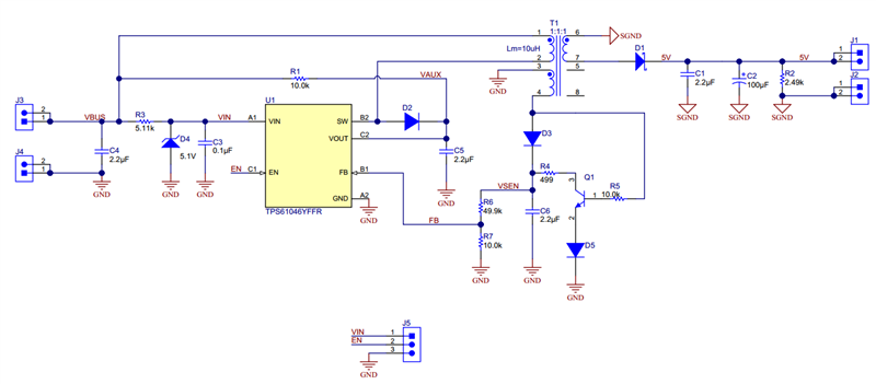
The reference design is based on flyback topology using the TPS61046, as shown in Figure 2. The TPS61046 is a 28V output, 900mA switch current boost converter. You can replace it with the TLV61046A small-outline transistor (SOT) package if you prefer.
The transformer supports up to a 4,000V isolation voltage. It has an auxiliary winding to sense the output voltage on the primary side. Ideally, the voltage in the VSEN node is almost the same as in the 5V node; thus, you can regulate the output voltage by regulating the VSEN. The method is called “primary-side regulation.” Compared to the method that senses the voltage directly in the secondary side, the benefit of primary-side regulation is that the optocoupler and reference voltage integrated circuit (IC) are not required, which greatly reduces the solution cost.
 Figure 2 A Schematic of a Primary-side
Regulation Flyback
Figure 2 A Schematic of a Primary-side
Regulation FlybackHowever, the leakage inductance of a nonideal transformer can cause the output voltage to go out of regulation when the load changes. This leakage inductance is inevitable for a real transformer. Methods to optimize the leakage inductance, such as a better magnetic core or special winding arrangement, will result in increased transformer cost.
The leakage inductance also causes extra current flowing into the VSEN node. As the TPS61046 always regulates the VSEN to the set voltage, the voltage at the 5V node would be out of the 4.5V to 5.5V range required by the transceiver. To solve this problem, introducing a dummy load in the VSEN and 5V nodes absorbs the extra current caused by the leakage inductance. This dummy load is traditionally a fixed-value resistor. However, as the energy of the leakage inductance changes with the real load, the required dummy load should be small at a small real-load condition and large at a large-load condition. But you cannot easily optimize the fixed dummy load to make sure that the output voltage stays within 4.5V to 5.5V if the load varies from 0 to 200mA. Furthermore, the fixed dummy load will greatly reduce the efficiency of the converter in light-load conditions.
The TPS61046 integrates a power-save-mode feature that reduces the switching frequency during light-load conditions to improve efficiency. In heavy-load conditions, the device operates with a constant switching frequency. Using the power-save-mode feature adds a special circuit comprising R4, R5, Q1 and D5 (as shown in Figure 2) to solve to the load regulation problem.
The circuit adjusts the dummy load automatically according to the real load conditions. When the real load is small, the switching frequency and on-time of Q1 are small, so the dummy current is also small. When the real load increases, the switching frequency and on-time of Q1 increase, so the dummy current also increases. This self-adjustable dummy load helps improve load regulation and efficiency. Figure 3 and Figure 4 show the test data in the evaluation board of the reference design.
 Figure 3 Load Regulation at
Different Input Voltages
 Figure 4 Efficiency at Different
Input Voltages
Figure 4 Efficiency at Different
Input VoltagesBeyond the TPS61046, you can use almost all boost converters to build an isolated flyback converter. You just need to select a suitable boost converter based on the input voltage, output voltage and output current, and solution cost.
Additional Resources
- Find more boost converters in the DC/DC boost converter selection page.
- Post a question in the TI E2E™ Community Non-Isolated DC/DC forum.
- Download the TPS61046 and TLV61046A data sheets.