SSZT955 september 2017 CSD88584Q5DC , CSD88599Q5DC
Appliances like power tools, garden tools and vacuum cleaners use low-voltage (two- to 10-cell) lithium-ion battery-powered motor drives. These tools use brushed DC (BDC) or three-phase brushless DC (BLDC) motors. BLDC motors are more efficient and have less maintenance, less noise and longer life spans.
The most important performance requirements of the power stage driving the motors are small form factor, high efficiency, good thermal performance, reliable protection and peak-current capability. A small form factor enables flexible mounting of the power stage inside the tool, better board layout performance and low-cost designs. High efficiency provides maximum battery life and reduces cooling efforts. Reliable operation and protection facilitate long lifetimes, which help with product reputations.
To drive a BDC motor in both the directions, you need to provide two half bridges (four metal-oxide semiconductor field-effect transistors (MOSFETs)) forming a full bridge. To drive a three phase BLDC motor, you need three half bridges (six MOSFETs) forming a three phase inverter.
With TI’s CSD88584Q5DC and CSD88599Q5DC power blocks, available in a small-outline no-lead (SON), 5mm-by-6mm package using a stacked die architecture, you can drive a BDC motor in both directions with just two power blocks and three-phase BLDC motor with just three power blocks , as shown in Figure 1. Each power block has two MOSFETs connected as a high side and low side MOSFET forming a half bridge.
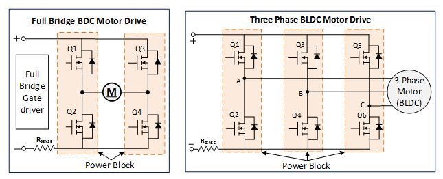 Figure 1 Power Block MOSFETs in
Different Motor-drive Topologies
Figure 1 Power Block MOSFETs in
Different Motor-drive TopologiesLet’s look at the benefits that these power blocks could bring to a cordless tool motor-drive subsystem design.
Double the Power Density
Clean MOSFET Switching with Low Parasitics
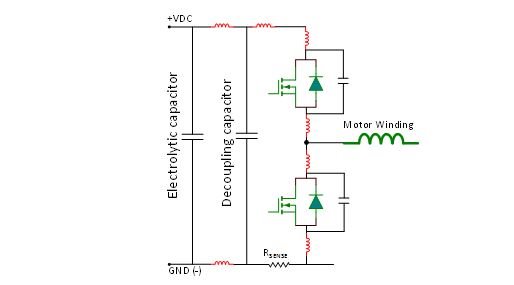 Figure 2 Parasitic Inductance and Capacitance in a Power Stage Half Bridge.
One of the causes of ringing is diode reverse recovery. A high rate-of-change of current caused by fast switching can result in a high diode reverse-recovery current. The reverse-recovery current flows through the parasitic layout inductance. The resonant network formed by the FET capacitance and the parasitic inductance cause phase-node ringing, reducing the voltage margin and increasing stress on the device. Figure 3 shows phase-node voltage ringing with discrete MOSFETs as a result of circuit parasitics.
With power blocks, having the switch-node clip that connects the two MOSFETs keeps parasitic inductances between the high and low MOSFETs to an absolute minimum. The use of a low- and high-side FET in the same package minimizes PCB parasitics and reduces phase-node voltage ringing.
Using these power blocks helps to ensure smooth MOSFET switching without voltage overshoots even at currents as high as 50A, as shown in Figure 4.
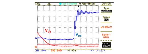 Figure 3 Phase-node Voltage Ringing and Voltage Overshoot with Discrete MOSFETs
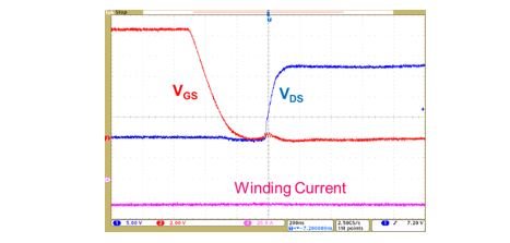 Figure 4 Clean Phase-node Switching Waveform with Power Blocks
Low PCB Losses with Reduced PCB Parasitic Resistance
If the design has a PCB copper thickness of 2oz (70µm), a single-layer PCB track connecting the phase node as given in Figure 5, will have approximately 0.24mΩ resistance. Assuming that the track exists in two PCB planes, the equivalent PCB resistance is 0.12mΩ. For a three phase power stage, you have three such PCB tracks. You can perform a similar analysis for the DC supply incoming and return tracks also.
The power block, having the top side and bottom side MOSFET in single package and the phase node connected by a metallic clip inside the package, optimizes the parasitic resistances and gives you the flexibility for layout and saves a minimal 0.5 to 1mΩ total PCB resistance.
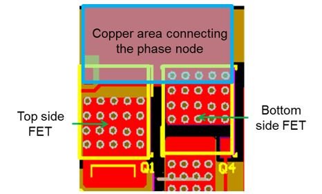 Figure 5 Typical Phase-node Track Length with Discrete MOSFETs
Superior Thermal Performance with Dual Cooling
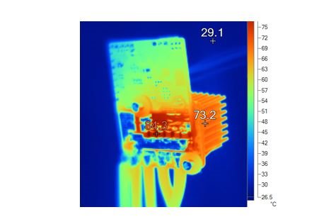 Figure 6 Thermal Image of the Board Showing Effective Top-side Cooling
In Figure 6, you can see the effectiveness of top-side cooling where the difference between the maximum temperature observed on the PCB (below the power block bottom case) and the heat sink temperature is less than 11°C. The heat is well conducted and distributed to the top-side heat sink through the top cooling metal pad of the power block.
Heat Sharing between the Top and Bottom FETs
- Use a different cooling area for the MOSFETs and provide more PCB copper area or heat sink for the MOSFET that has more losses.
- Use different devices for the top- and bottom-side MOSFETs depending on their nominal current. For example, you can use a device with less ON state conduction resistance (RDS_ON) for the MOSFET that carries more current.
These methods will not give optimal cooling when the MOSFET heat up depends on the operating duty cycle, resulting in underutilization of the PCB area or MOSFET rating. Using power block MOSFETs, where the top and bottom MOSFETs are in the same package, results in automatic heat sharing between the top- and bottom-side MOSFETs and provides both better thermal performance and optimized system performance.
Low System Cost
- Half the solution size, reducing PCB cost drastically.
- Low parasitics enable a much more reliable solution, one with longer life and low maintenance.
- Reducing the PCB track length reduces the PCB resistance, resulting in lower losses and higher efficiency with a smaller heat sink.
- Superior thermal performance resulting in less cooling efforts.
A MOSFET power block helps to achieve a more reliable, smaller-sized, efficient and cost-competitive system solution.
Additional Resources
- Check out our latest reference design that utilizes TI’s 40-V MOSFET power block technology
- Learn how our compact 1kW power stage reference design achieves 99% efficiency for 36V brushless DC (BLDC) motors
- Read about how the demand for higher power density is driving innovation
- Learn more about power MOSFET modules from TI