-
Making Trade-offs When Integrating Input and Output Capacitors in a DC/DC Step-down Power Module
Making Trade-offs When Integrating Input and Output Capacitors in a DC/DC Step-down Power Module
The ideal goal of a DC/DC step-down (buck) point-of-load power module is to integrate the entire bill of materials (BOM) inside the package. In reality, most power modules require several external components, including input and output capacitors. These capacitors are usually external because they are too expensive and bulky to integrate in the package.
A high-switching-frequency buck architecture will minimize both the size and amount of external capacitors. But while these architectures shrink the BOM to enable integration in the module, you will have to make trade-offs in performance and operating range.
Take for example the TPSM84A21, a 10A DC/DC power module that uses a high-frequency two-phase architecture and switches at 4MHz. The TPSM84A21 integrates 66.1µF of input capacitance and 185µF of output capacitance, a regulator IC, two inductors, and passives in a 9mm-by-15mm-by-2.3mm package. The only external component required is a single programming resistor. For comparison, the LMZ31710 is a 10A DC/DC power module in a 10mm-by-10mm-by-4.3mm package that switches at 500kHz and requires significantly more capacitance than the TPSM84A21, all external to the module. Table 1 compares the capacitance.
| TPSM84A21 | LMZ31710 | |
|---|---|---|
| Input capacitance | Internal: 66.1µF ceramic | External: 100µF tantalum 47.1µ ceramic |
| Output capacitance | Internal: 185µF | External: 200µF tantalum 220µF ceramic |
Let’s take a further look at how these two solutions compare in specs, solution size, efficiency, transient response and electromagnetic interference (EMI) performance.
Spec and Feature Comparison
The TPSM84A21 output range is from 0.55V to 1.2V. The TPSM84A22 is required for output voltages from 1.2V to 2.05V. In comparison as seen in Table 2, the LMZ31710 input range is wider and covers output voltages from 0.6V to 3.6V with a single device.
| TPSM84A21 | LMZ31710 | |
|---|---|---|
| Minimum input voltage (V) | 8V | 4.5V (2.95V with external bias) |
| Maximum input voltage (V) | 14V | 17V |
| Minimum output voltage (V) | 0.55V 1.2V (TPSM84A22) | 0.6V |
| Maximum output voltage (V) | 1.35V 2.05V (TPSM84A22) | 3.6V |
| Maximum output current (A) | 10A | 10A |
| Typical switching frequency | 4MHz | 500kHz |
| Power good | Y | Y |
| Adjustable soft start | N | Y |
| Current sharing | N | Y |
| Adjustable current limit | Y | Y |
| Frequency synchronous input | Y | Y |
| Frequency synchronous output | N | Y |
Solution Size
Figure 1 shows that although the TPSM84A21 package is larger, the overall solution area is 60% smaller.
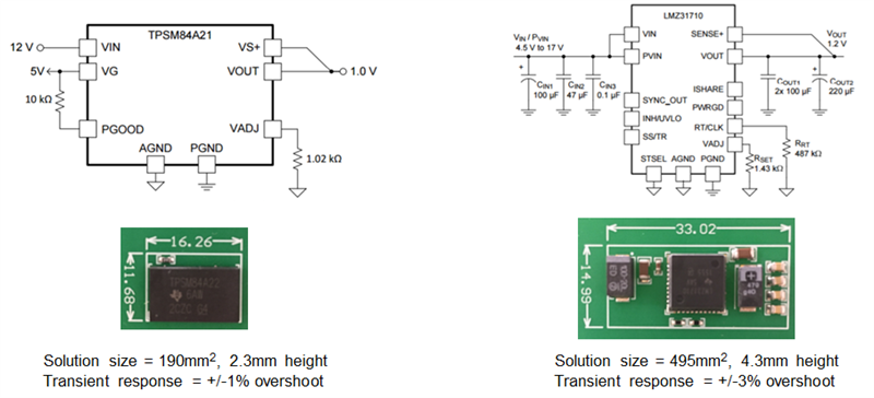 Figure 1 Solution-size Comparison
Efficiency
Figure 2 shows that the efficiency of the LMZ31710 is much greater at low to mid loads; however, at full load the efficiency is similar to a 12V-to-1.2V conversion.
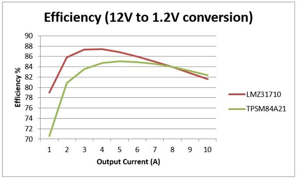 Figure 2 Efficiency Comparison for a
12V-to-1.2V Conversion
Figure 2 Efficiency Comparison for a
12V-to-1.2V ConversionFigure 3 shows how the efficiency of the TPSM84A22 and LMZ31710 are similar for a 12V-to-1.8V conversion.
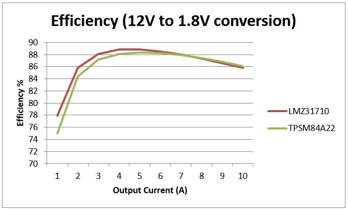 Figure 3 Efficiency Comparison for a
12V-to-1.8V Conversion
Figure 3 Efficiency Comparison for a
12V-to-1.8V ConversionTransient Response
As you can see in Figure 4, the TPSM84A21’s transient response is considerably better in a worse-case condition, with no external output capacitance.
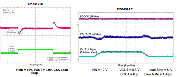 Figure 4 Transient Response Comparison
Radiated EMI
In Figure 5, the radiated EMI of both the TPSM84A22 and LMZ31710 meet Comité International Spécial des Perturbations Radioélectriques (CISPR) 22 Class B radiated EMI, but the LMZ31710 has lower peak emissions.
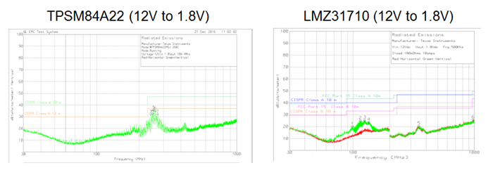 Figure 5 Radiated EMI
Comparison
Figure 5 Radiated EMI
ComparisonConclusion
Integrating the input and output capacitors in a small footprint requires a high-switching-frequency architecture, which significantly reduces the overall solution size and transient response and makes the design incredibly simple. The trade-off is a narrower operating input and output voltage range, lower efficiency in some conditions, and higher peak-radiated EMI. With a traditional current-mode buck architecture, the operating range is wider, offering good efficiency and more features. Depending on the situation, both the TPSM84A21/2 and LMZ31710 are excellent options for point-of-load applications.
Additional Resources
- Read the blog post, “Step by step: How the series capacitor buck converter works.”
- Start a design now with WEBENCH® power designer.
- Order the TPSM84A21 10A SWIFT™ power module evaluation module.
IMPORTANT NOTICE AND DISCLAIMER
TI PROVIDES TECHNICAL AND RELIABILITY DATA (INCLUDING DATASHEETS), DESIGN RESOURCES (INCLUDING REFERENCE DESIGNS), APPLICATION OR OTHER DESIGN ADVICE, WEB TOOLS, SAFETY INFORMATION, AND OTHER RESOURCES “AS IS” AND WITH ALL FAULTS, AND DISCLAIMS ALL WARRANTIES, EXPRESS AND IMPLIED, INCLUDING WITHOUT LIMITATION ANY IMPLIED WARRANTIES OF MERCHANTABILITY, FITNESS FOR A PARTICULAR PURPOSE OR NON-INFRINGEMENT OF THIRD PARTY INTELLECTUAL PROPERTY RIGHTS.
These resources are intended for skilled developers designing with TI products. You are solely responsible for (1) selecting the appropriate TI products for your application, (2) designing, validating and testing your application, and (3) ensuring your application meets applicable standards, and any other safety, security, or other requirements. These resources are subject to change without notice. TI grants you permission to use these resources only for development of an application that uses the TI products described in the resource. Other reproduction and display of these resources is prohibited. No license is granted to any other TI intellectual property right or to any third party intellectual property right. TI disclaims responsibility for, and you will fully indemnify TI and its representatives against, any claims, damages, costs, losses, and liabilities arising out of your use of these resources.
TI’s products are provided subject to TI’s Terms of Sale (www.ti.com/legal/termsofsale.html) or other applicable terms available either on ti.com or provided in conjunction with such TI products. TI’s provision of these resources does not expand or otherwise alter TI’s applicable warranties or warranty disclaimers for TI products.
Mailing Address: Texas Instruments, Post Office Box 655303, Dallas, Texas 75265
Copyright © 2023, Texas Instruments Incorporated