SSZTA06 july   2017 UCD9090 , UCD9090A


  1.   1
  2.   2
    1.     3
    2.     What Is a Fault Pin?
    3.     What Is the GPI Fault Response?
    4.     What Is GPI Debugging?
    5.     What Is the LGPO Sequencing On/off Dependency?
    6.     What Is the Rail State?
    7.     What Is Cold Boot Mode?
    8.     Will TI Continue to Offer the UCD9090?
    9.     Migrating from the UCD9090 to UCD9090A

Electronic systems that include a central processing unit (CPU), digital signal processor (DSP), microcontroller (MCU), field-programmable gate array (FPGA) or application-specific integrated circuit (ASIC) can have multiple voltage rails and require certain power on/off sequences in order to function correctly. TI’s UCD9090A power-supply sequencer and monitor with Advanced Configuration and Power Interface (ACPI) support can control up to 10 voltage rails, ensures correct power sequences during both normal and fault conditions, and includes a dedicated fault pin to easily cascade multiple devices.

The UCD9090A is an upgrade to the former UCD9090 (listed as not recommended for new designs [NRND]). In this post, I will explain the differences between the two devices, including their operation and features, and how to migrate from the UCD9090 to the UCD9090A.  Table 1 lists the features included with the new UCD9090A.

Table 1 Comparison of Features of the UCD9090 and UCD9090A
Features UCD9090A UCD9090
Fault pin (enables single to cascading multiple UCD9090A devices) Yes No
General Purpose Input (GPI) fault response Yes No
GPI debugging Yes No
Rail state Yes No
Fault/peak logging disable Yes No
Logic General Purpose Output (LGPO) sequence on/off dependency Yes No
Non-volatile (NV) fault log 26 30
Rail sequence on/off timeout 140m 32s
Cold boot mode Yes No

What Is a Fault Pin?

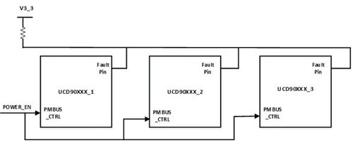
The fault pin is a new feature that enables you to cascade multiple TI UCD9090A devices with fault-pin capability. The fault pin is a bidirectional signal connected to a fault bus. The fault bus is pulled up to 3.3V by a 10K resistor. When no fault exists on a particular UCD9090A device, the fault pin is a digital input pin that listens to the fault bus. When one or multiple UCD9090A devices detect a rail fault, the corresponding fault pin turns to the active driven low state, pulling down the fault bus and informing all other UCD9090A devices of the corresponding fault. This way, coordinated action can occur across multiple devices. After the fault is cleared, the state of the fault pin turns back to an input pin. A diagram showing use of a fault pin is show in Figure 1.

GUID-BF09A467-7CBB-4FB6-B1D7-5C85D3D28E56-low.jpg Figure 1 Example Using a Typical Fault Pin

What Is the GPI Fault Response?

This feature solves the issue of limited Analog Monitor (AMON) pins. For example, in the UCD9090, when all 10 rails are assigned to a voltage monitor; the system does not have the capability to monitor one more external event (e.g., OVER_TEMP) or one more rail. With the GPI fault response feature in place, the external event or POWER_GOOD of the point of load (POL) could connect to the assigned GPI. When the signal changes to de-asserted, the UCD9090A can help shut down the rails and retry and re-sequence the system based on how the GPI fault-response is configured.

What Is GPI Debugging?

To avoid triggering the PMBus alert, response fault or continue system watchdog during board-level debug or programming, a GPI pin can be assigned to perform a GPI debugging function on the UCD9090A. When asserting the assigned GPI, the device is under the GPI debug mode. The device will not activate the PMBus alert pin for any faults/warnings nor respond to any fault response. It will not log any faults, will suspend system watchdog and ignore the sequencing dependencies for rails.

What Is the LGPO Sequencing On/off Dependency?

The UCD9090 only supports sequencing dependencies over rail and GPI. If users want to have sequencing dependencies on the LGPO, they have to physically wire the LGPO signal back to one of the GPIs. This approach requires two extra pins which could be an issue for applications that have limited pins available. The LGPO sequencing dependency feature was introduced with the UCD9090A to save the two extra pins for other functions.

What Is the Rail State?

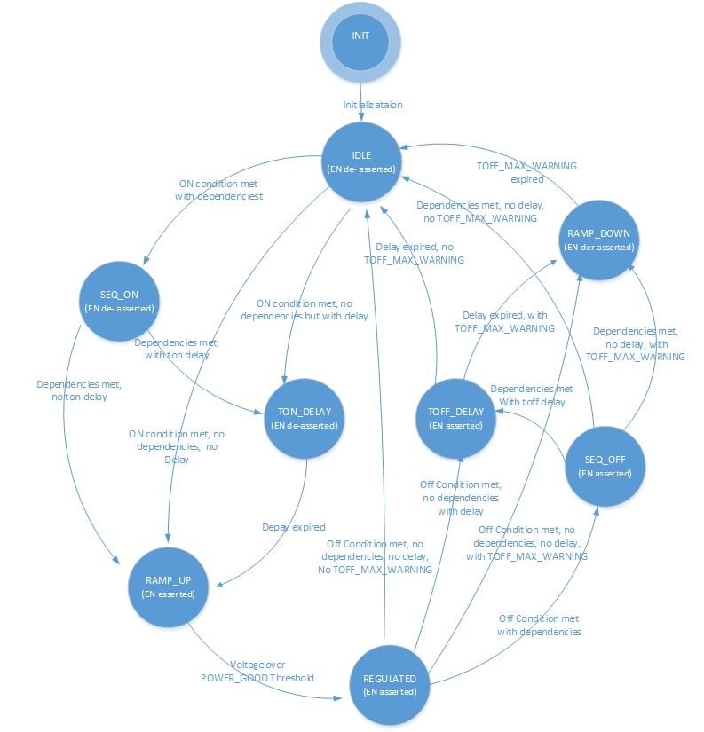
Each device has up to nine states: INIT, IDLE, SEQ_ON, TON_DELAY, RAMP_UP, REGULATED, SEQ_OFF, TOFF_DELAY and RAMP_DOWN. The state of the rail can help you easily determine the status of the system so that you can more easily bring up or debug the power system. Figure 2 shows how the rail states are changed.

GUID-C2A1E411-BB2F-4A89-9A00-55CAC77DBC49-low.jpg Figure 2 Rail State Machine Diagram

What Is Cold Boot Mode?

Cold boot is a feature specifically designed for cold-temperature applications like telecom. It has the intelligence to heat up a system by turning on the cold boot rails for certain amounts of time when it is experiencing extremely cold temperatures. The UCD9090A device communicates with the system through a particular GPI called the thermal-state GPI, which is a digital output from a thermal sensing device. The cold boot feature is fully configurable, enabling you to select enable/disable, the number of cold boot rails and the timeout period. Figure 3 is a pseudo processing call of how cold-boot is handled by the device.

GUID-654F60E9-9452-4D38-8F35-401A916BBFD5-low.png Figure 3 Cold-boot Processing Call

Will TI Continue to Offer the UCD9090?

Having these new features makes the UCD9090A a better candidate over the UCD9090 for various applications, but note that TI will continue supporting and building the UCD9090 until it reaches ten consecutive years of no sales.

Migrating from the UCD9090 to UCD9090A

The UCD9090 and UCD9090A are pin-to-pin compatible devices. The UCD9090A supports all features of the UCD9090. Moving to the UCD9090A does not require any schematic changes. Moreover, you can seamlessly import the project file (.xml) file generated from the UCD9090 into the UCD9090A with TI’s Fusion Digital Power Designer TM GUI to help reduce the migration effort.

Because of the new features, the script file (.csv) and data flash image file (.hex, .x0) are not compatible between the UCD9090 and UCD9090A. You cannot import files generated from the UCD9090 into the UCD9090A because the device will not function as expected. To use script file or data flash image file on the UCD9090A, follow these steps:

  1. Install www.ti.com/tool/fusion_digital_power_designer and open the latest Fusion Digital Power Designer GUI.
  2. Import the old UCD9090 project (.xml) into the UCD9090A. See Figure 4.
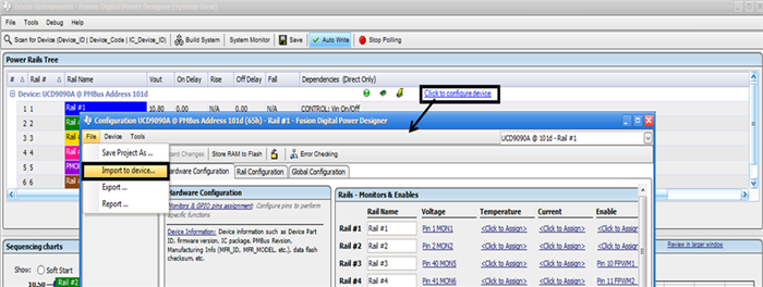
GUID-D382D59C-5844-41C8-A588-DF34C2797A5B-low.png Figure 4 Import the UCD9090 Project File

3. Once you have successfully imported the project, use the export function from the Fusion Digital Power Designer GUI to regenerate the .csv/.hex file. See Figure 5.
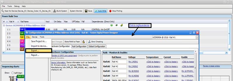
GUID-F65E2FDD-5517-40FF-8DE2-A45F98465AF0-low.png Figure 5 Fusion Digital Power Designer GUI Export Settings

4. Use the .csv/.hex file generated from step No. 3 for any programming utilities.

Hopefully this blog post provides you with a good comparison between the two devices and will help you migrate from the UCD9090 to the UCD9090A. If you have any additional questions, please post a response below or submit through TI’s E2E™ Community Sequencers forum.