-
Powering the Next Generation of Home Appliances: How to Get More from Less
Powering the Next Generation of Home Appliances: How to Get More from Less
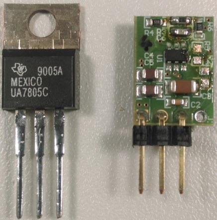
 Figure 1 High-efficiency 5V,
1A Switch-mode Power Supply Design in a T0-220 Form Factor
Figure 1 High-efficiency 5V,
1A Switch-mode Power Supply Design in a T0-220 Form Factor“Get more from less” – that is always the goal, and it is especially true for power consumption in appliances. As a designer, your goal is to get more current to power more subsystems, while decreasing overall power consumption.
It’s trendy to add new functionality into home appliances, like having a washing machine send a message when the washing cycle is finished, or a refrigerator displaying what is inside, either on a screen or by emailing a picture. These additional features need new subsystems like wireless communication, sensors, human-machine-interface (HMI) and lighting, which all need power.
At the same time, appliances need to consume as little power as possible in order to limit their impact on the environment, reduce electricity costs for consumers, and successfully pass more and more stringent energy ratings.
Additionally, cost, size and reliability are always key requirements.
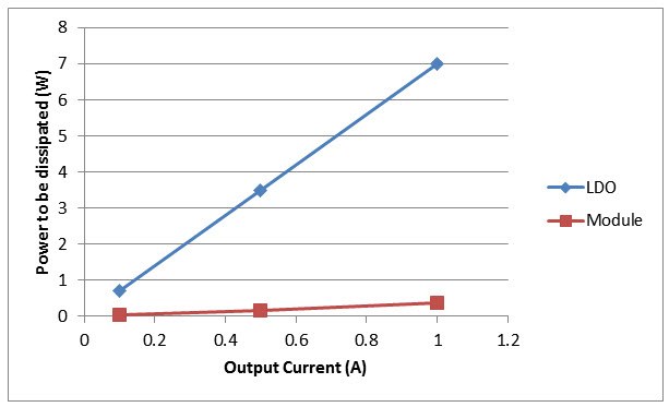
Low-dropout regulators (LDOs) are traditionally used in home appliances to generate 5V or 3.3V from the 12V rail. But LDOs have really poor efficiency. Figure 2 compares the power dissipated for a 12V-input and 5V-output in an LDO and a high efficiency DC/DC switch-mode power supply (SMPS) reference design in a TO-220 form factor versus output current.
 Figure 2 Power Dissipated by a LDO and
a DC/DC Switch-mode Power Supply versus Output Current
Figure 2 Power Dissipated by a LDO and
a DC/DC Switch-mode Power Supply versus Output CurrentAs expected, the LDO has poor efficiency, which is why its maximum output current is limited; it also requires a bulky heat sink to dissipate the losses. A heat sink is not required in a DC/DC converter, and all four reference designs include the TPS54202 step-down converter.
You could use a DC/DC converter to convert the 12V to 5V or 3.3V, achieving higher efficiency and higher current drive capability to power multiple new subsystems. Moreover this would decrease the input current consumed, which will help the appliance pass strict energy ratings.
TI has four reference designs to address these issues:
- 5V 1A, Low EMI, 94% Efficiency DC/DC SMPS in Dual Layer TO-220 Form Factor Reference Design.
- 3.3V 1A, Low EMI, 92% Efficiency DC/DC SMPS in Dual Layer TO-220 Form Factor Reference Design.
- 5V 1A, Low EMI, 94% Efficiency DC/DC SMPS in Single Layer TO-247 Form Factor Reference Design.
- 3.3V 1A, Low EMI, 92% Efficiency DC/DC SMPS in Single Layer TO-247 Form Factor Reference Design.
All four SMPS reference designs are pin-to-pin compatible with the TO-220 package traditionally used for LDOs in appliances, thus enabling quick evaluation by swapping the LDO with the DC/DC reference design and saving both time and cost during the evaluation/redesign phase.