SSZTAT5 october 2016
When I studied electrical engineering at the university, math was extremely important. My math professor was so diligent that he would attend other classes to see if the lessons involved math that he needed to teach us to make our lives easier. More than once he changed his lesson plans to incorporate math topics from the other classes, so I was very grateful that he was so passionate.
When I became an application engineer for power supplies, I quickly learned that there are parasitics in all components. The formulas to calculate the best-fitting component became more and more complicated when including these parasitics. Sometimes a simplified formula or even a rule of thumb helped me get at least close to a result, enabling me to find the best-fitting available component through trial and error.
One issue where I could never use math, however, was when deciding about the best layout. I still don’t have a really good simulation tool that can predict exactly which layout is the best fit for the specific power supply I want to design. My dilemma gets even worse if the IC includes several converters, like LCD (Liquid Crystal Display) or OLED (Organic Light Emmiting Diode) display power products. The parasitics of a layout not shown in the schematic do influence the performance of a circuit and can even cause hazardous failures in a power supply. So it is important to do the layo=ut right the first time.
One parasitic effect to keep in mind when doing a layout is the trace or plane resistance. Here is a rule of thumb that I’ve learned to estimate it: count squares.
I learned about this rule the first time I laid out a power-supply design. I remember being somewhat puzzled because I could not believe that it could be so simple, but it is; I even can use math to show you that it’s true.
Figure 1 calculates the resistance of copper:
") Figure 1 (1)
Figure 1 (1)Figure 2 shows a piece of copper on top of a printed circuit board (PCB).
 Figure 2 Copper Piece Carrying Current
in a Power-supply Design
Figure 2 Copper Piece Carrying Current
in a Power-supply DesignAssume the current is flowing from left to right along l and distributes evenly in area A. In this case, Figure 1 becomes Figure 1:
") Figure 3 (2)
Figure 3 (2)You can see now that the resistance of this piece of copper is independent of the dimension l . So now the formula for resistance on a PCB changes to Figure 1:
") Figure 4 (3)
Figure 4 (3)Where ρ is the well-known specific copper resistance and the production specification of the PCB defines the thickness of the copper.
This means that regardless of how big l is, the resistance stays the same. For a layout person this is really good to know, because if you want to make the resistance as small as possible, make it as wide and as short as possible.
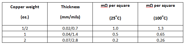
You can determine the thickness of copper on a PCB from the requested production parameter (see Table 1) and estimate the resistance of a specific piece of copper in the layout by counting squares.
|
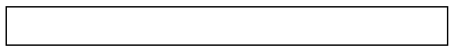
Assume your piece of wire looks like the following:
Divide it into squares, as shown here:
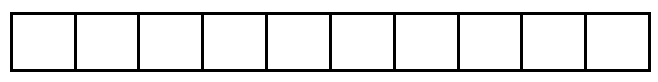
Say that you can fit 10 squares into your piece of wire, like in the above diagram. If you are using 1oz copper on your PCB, the resistance of this piece of wire is roughly 5mΩ. If a current of 1A is going through this piece of wire, the voltage drop from one end to the other end will be 5mV. Assuming a voltage of 1V on one end, the voltage on the other end is 0.5% smaller – and this is just one piece of wire. Double the width of your wire and you halve the resistance.
So even if it is relatively easy to calculate the parasitic resistance, using my eyes and estimating the number of squares that fit into the wire made it a lot easier for me. Let me know how this works for you in the comments below! Check out the LCD/OLED display bias solutions offered by TI and share your results in the LCD/OLED Display Bias Solutions forum on the TI E2E™ Community.