Eye Doctor: Why Too Much Equalization Boost Is Bad for Your Serial Link Health
Welcome to the “Eye Doctor” series! This post will walk through challenges that signal integrity and hardware engineers face when designing or debugging multi-gigabit per second links. Whether you are working on next generation high resolution video displays, medical imaging, data storage or the latest high speed Ethernet and tele-communications protocols, we all face the same basic signal integrity challenges. Let’s kick off the series by talking about over-equalization.
Serializers and deserializers (SERDES) in modern application-specific integrated circuits (ASICs) and field-programmable gate arrays (FPGAs) are typically capable of achieving good link performance across channels with loss up to 30dB. Channels that are a bit longer or higher in loss often require assistance from signal conditioners such as retimers or repeaters. These devices compensate for the effects of long channels and provide systems the margin necessary to drive extra-long distances.
One of the primary functions for a repeater or retimer is to compensate for the insertion loss of the channel. This function breaks down to receive equalization and transmit equalization. Receive-equalization circuits typically consist of a continuous time linear equalizer (CTLE) and sometimes a decision feedback equalizer (DFE). De-emphasis or finite impulse response filters (FIR) are common options for transmit-equalization circuits. Receive-equalization circuits apply boost to the signal after a long channel to compensate for frequency-dependent loss. Transmit-equalization circuits change the shape of the launch signal so that the signal will recover more easily after its attenuation by traveling across the channel.
For both receive equalization and transmit equalization, it is important to apply the appropriate amount of equalization. Applying too little equalization (under-equalization) can prevent the signal from being recovered properly. However, applying too much equalization (over-equalization) can also be an issue because over-equalized waveforms can interfere with the receiver’s ability to recover the data.
Figure 1 shows two example eye diagrams. One eye diagram is properly tuned for the channel (left), while the other shows signs of over-equalization (right).
 Figure 1 Properly Tuned versus
Over-equalized Eye Diagrams
Figure 1 Properly Tuned versus
Over-equalized Eye DiagramsThe largest difference between the two eye diagrams is at the 0V crossing. The over-equalized eye diagram on the right shows separation of the rising and falling edges. This is commonly referred to as “double banding.” Double banding can interfere with a receiver’s ability to properly detect the frequency or maintain the proper phase relationship with incoming data.
Using the jitter decomposition function of an oscilloscope, you can see in Figure 2 how the over-equalized eye shows bimodal jitter content. In other words, the jitter distribution is on two frequencies that average out to the data rate rather than the actual data rate itself. Further examination shows that this bimodal jitter distribution is associated with data-dependent jitter, which is directly impacted by the amount of equalization applied by the equalizer.
 Figure 2 Jitter Decomposition of
Properly Tuned versus Over-equalized Eye Diagrams
Figure 2 Jitter Decomposition of
Properly Tuned versus Over-equalized Eye DiagramsOver-equalization can present itself in many ways; Figure 3 shows a more classic case. The scope shots on the left show a properly equalized eye. The over-equalized plots shown on the right exhibit both double-banded eye diagram edges and excessive amplitude on bit transitions. In this case, the extra amplitude on the bit transitions could lead to compliance issues with system specifications for logic-high and logic-low level tolerances. Also note the differences between the jitter profiles.
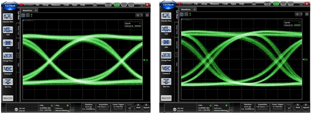
 Figure 3 Alternate Presentation of
Over-equalization – Double Banding with Overshoot
Figure 3 Alternate Presentation of
Over-equalization – Double Banding with OvershootWhen tuning or optimizing links for best performance, keep in mind both the horizontal and vertical eye opening. It is easy to maximize for one or the other, but be sure to avoid over-equalizing the signal, as that may increase the bit error rate. In my next installment, I’ll be discussing reflections – what are they, and how engineers can mitigate their effects in their high-speed systems. Subscribe to Analog Wire to receive an email notification upon the publication of the second post.
What considerations do you face when optimizing links for best performance? Log in and leave a comment below.
Additional Resources
IMPORTANT NOTICE AND DISCLAIMER
TI PROVIDES TECHNICAL AND RELIABILITY DATA (INCLUDING DATASHEETS), DESIGN RESOURCES (INCLUDING REFERENCE DESIGNS), APPLICATION OR OTHER DESIGN ADVICE, WEB TOOLS, SAFETY INFORMATION, AND OTHER RESOURCES “AS IS” AND WITH ALL FAULTS, AND DISCLAIMS ALL WARRANTIES, EXPRESS AND IMPLIED, INCLUDING WITHOUT LIMITATION ANY IMPLIED WARRANTIES OF MERCHANTABILITY, FITNESS FOR A PARTICULAR PURPOSE OR NON-INFRINGEMENT OF THIRD PARTY INTELLECTUAL PROPERTY RIGHTS.
These resources are intended for skilled developers designing with TI products. You are solely responsible for (1) selecting the appropriate TI products for your application, (2) designing, validating and testing your application, and (3) ensuring your application meets applicable standards, and any other safety, security, or other requirements. These resources are subject to change without notice. TI grants you permission to use these resources only for development of an application that uses the TI products described in the resource. Other reproduction and display of these resources is prohibited. No license is granted to any other TI intellectual property right or to any third party intellectual property right. TI disclaims responsibility for, and you will fully indemnify TI and its representatives against, any claims, damages, costs, losses, and liabilities arising out of your use of these resources.
TI’s products are provided subject to TI’s Terms of Sale (www.ti.com/legal/termsofsale.html) or other applicable terms available either on ti.com or provided in conjunction with such TI products. TI’s provision of these resources does not expand or otherwise alter TI’s applicable warranties or warranty disclaimers for TI products.
Mailing Address: Texas Instruments, Post Office Box 655303, Dallas, Texas 75265
Copyright © 2023, Texas Instruments Incorporated