SSZTBG1 april 2016
As the demand for automotive and industrial power increases, so does the need for multiphase and modular-based designs. Designing a multiphase or multimodule board can be tedious and take a long time. In this Altium tips blog, I will show you how to easily copy and paste an existing schematic and layout to create a multiphase or multimodule designs.
Step No. 1: Build a simple buck-converter schematic in Altium (Figure 1).
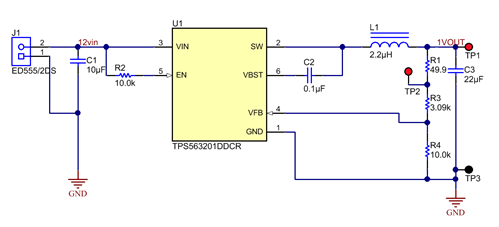 Figure 1 Altium Schematic
Step No. 2: Update the printed circuit board (PCB) and layout the components. Pour the polygon pours as normal and connect all of the nets (Figure 2).
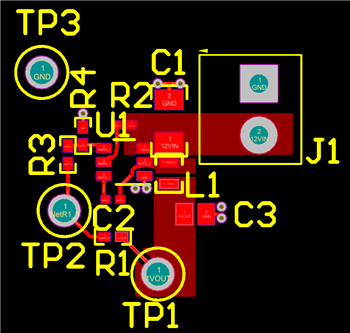 Figure 2 Layout in Altium
Step No. 3: Select the components you want to copy by clicking and dragging; then right-click and select Copy (Figure 3).
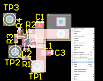 Figure 3 Screenshot of Step No.
3
Figure 3 Screenshot of Step No.
3After copying, Altium will ask for a reference point; click a specific component.
Step No. 4: Paste the new components next to the existing components, as shown in Figure 4. Altium will add “_1” next to each reference designator to signify that it’s a copied component.
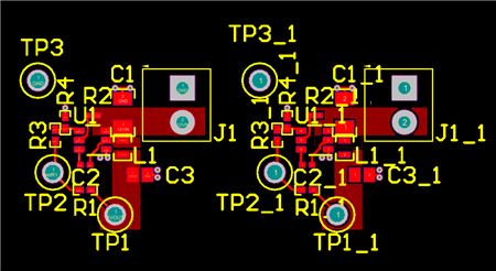 Figure 4 Layout in Altium Showing
Copied Components
Figure 4 Layout in Altium Showing
Copied ComponentsNow that you’ve successfully copied the components into the layout, you’ll need to do the same in the schematic window and then link the components.
Step No. 5: In the Projects window, right-click the project name and click Add New to Project; then click Schematic (Figure 5). This will give you a new schematic sheet to copy components into.
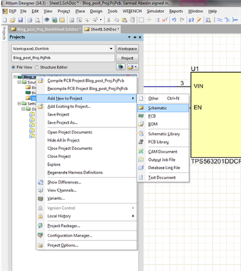 Figure 5 Screenshot of Step No.
5
Figure 5 Screenshot of Step No.
5Step No. 6: Copy and paste the schematic in Figure 1 to the new sheet. You will have to add “_1” to all of your new components before you can link the schematic with the current layout. To do that, you can use the Smart Edit option in Altium.
Step No. 7: Right-click U1 (new sheet) and select Find Similar Objects (Figure 6). Click OK in the pop-up menu.
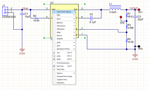 Figure 6 Screenshot of Step No.
7
Figure 6 Screenshot of Step No.
7Altium will highlight all of the components on the schematic and open the SCH Inspector window.
Step No. 8: Click the “…” button to the right of Component Designator (Figure 7).
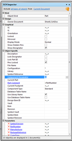 Figure 7 Screenshot of Step No.
8
Figure 7 Screenshot of Step No.
8Step No. 9: In the Smart Edit window, click the Formula tab (Figure 8).
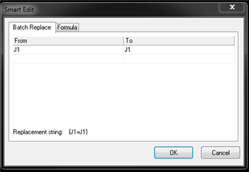 Figure 8 Screenshot of Step No.
9
Figure 8 Screenshot of Step No.
9Step No. 10: In the Apply formula field, type “! + '_1'” (no quotation marks) and click OK (Figure 9).
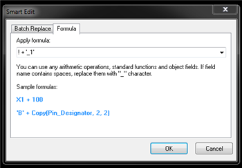 Figure 9 Screenshot of Step No.
10
Figure 9 Screenshot of Step No.
10Altium will add “_1” to the existing reference designators. This will now match your layout (Figure 10).
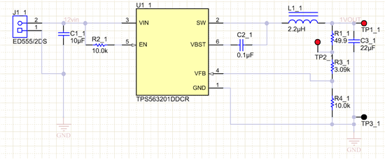 Figure 10 Revised Schematic
Step No. 11: While in the schematic window, update your PCB (Design > Update) to see the net(s) appear, as in Figure 11.
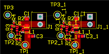 Figure 11 Revised Layout in
Altium
Figure 11 Revised Layout in
AltiumYou must also add “_1” to any nets where you don’t want the modules to share. Follow the same Smart Edit procedure.
Step No. 12: Right-click any net labels. Select Find Similar Objects and click OK (Figure 12). After Altium highlights all of the nets, click off of any nets you want the modules to share, like VIN, etc.
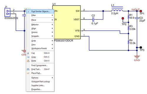 Figure 12 Screenshot of Step No.
12
Figure 12 Screenshot of Step No.
12Step No. 13: In the SCH Inspector window, click “…” to the right of Text (Figure 13).
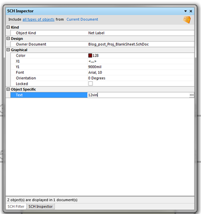 Figure 13 Screenshot of Step No.
13
Figure 13 Screenshot of Step No.
13Step No. 14: In the Smart Edit window, click in the Apply formula field and type ! + ‘_1’. Click OK (Figure 14).
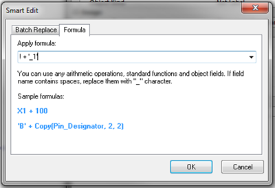 Figure 14 Screenshot of Step No.
14
Figure 14 Screenshot of Step No.
14All of the nets will now have “_1” next to them, signifying that they are from your original module. Your new schematic sheet will look like Figure 15.
 Figure 15 Revised Altium
Schematic
Figure 15 Revised Altium
SchematicStep No. 15: Update the PCB; you’ll see new net names (Figure 16). The only net shared between the two modules/phases is now the GND net.
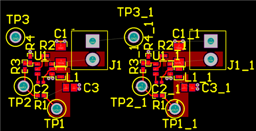 Figure 16 Revised Layout in
Altium
Figure 16 Revised Layout in
AltiumPolygon pours will copy over, but you will need to rename them to the new nets (Figure 17).
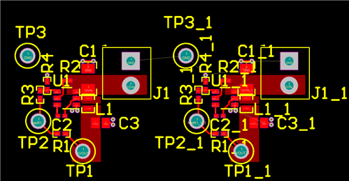 Figure 17 Revised Layout in
Altium
Figure 17 Revised Layout in
AltiumThese steps should save you substantial time when making multiphase or multimodular PCBs in Altium and help designers get their products to market faster.
With current-sharing designs in particular, the smallest of differences in layout can lead to nonequal sharing. So another great reason to use this copy-and-paste trick is that it helps reduce the small differences that can come from individual component placement.
Additional Resources
- Get more information on Altium Designer.
- Explore more power-supply topics.
- Watch Power Tips videos to help with your design challenges