-
Shrink Your LED Flash Solution
Shrink Your LED Flash Solution
John Woodward
You may have noticed that the screens are getting bigger on smartphones. But, the actual space inside the phones is shrinking, despite the fact that designers must deal with more parts – bigger batteries, more sensors, more processors. Tighter space restrictions and more parts are giving designers big headaches these days.

One feature built into TI’s newest LED flash driver family is helping designers reduce the size of the selfie flash, dual flash or torch (movie mode) LED application. Available in the LM3643, LM3644 and LM3648, this mode enables you to put the device in a forced flash mode.
 Figure 1 Boost Configuration
Register
Figure 1 Boost Configuration
RegisterIn Boost Configuration Register, a bit exists to control the mode of the boost, with options for normal mode and pass mode. In normal mode, the boost is operating as a standard boost converter. In pass mode, it is basically acting as an LDO. In the latter case, there is no need to connect the inductor.
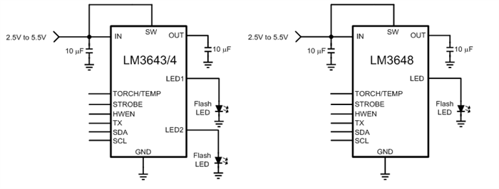
 Figure 2 Typical Circuits for Use
without Inductor
Figure 2 Typical Circuits for Use
without InductorInductor case sizes are decreasing as technology improves, but they still take up considerably more space in a typical solution than the rest of the bill of materials.
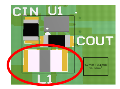
 Figure 3 Typical Layout of LM3643,
LM3644, and LM3648
Figure 3 Typical Layout of LM3643,
LM3644, and LM3648In this typical layout, shown in Figure 3, you can see that removing the inductor can improve the solution size by around 30%.
Realizing a smaller solution size without inductor is one thing, but can your application and design tolerate the use of an LED driver in pass mode all the time? That is the question you need to answer. The key is to verify the minimum input voltage and the maximum forward voltage of the LED when you are at the maximum current you intend to power the LED with. To do this, use the details in Equation 1:

where VHR and RDSONPMOS come from the device specification and the rest from your application design.
For example, if ILEDTOTAL = 200mA, RDSONPMOS = 90mΩ, VLED = 3V @ 200mA and VHR = 160mV:

So, for this example, as long as the input voltage of your application stays above 3.2V, you are good to go. The size savings are dramatic. The solution is simple. But take care to make sure that bit 2 of the boost configuration register is set to 1. Also, you must force pass mode at all times; damage will occur if you forget.
Now, go shrink your LED flash solution!
Additional Resources
- Check out TI’s camera flash LED driver solutions.
- Taking a selfie? Analog technology makes it possible.
IMPORTANT NOTICE AND DISCLAIMER
TI PROVIDES TECHNICAL AND RELIABILITY DATA (INCLUDING DATASHEETS), DESIGN RESOURCES (INCLUDING REFERENCE DESIGNS), APPLICATION OR OTHER DESIGN ADVICE, WEB TOOLS, SAFETY INFORMATION, AND OTHER RESOURCES “AS IS” AND WITH ALL FAULTS, AND DISCLAIMS ALL WARRANTIES, EXPRESS AND IMPLIED, INCLUDING WITHOUT LIMITATION ANY IMPLIED WARRANTIES OF MERCHANTABILITY, FITNESS FOR A PARTICULAR PURPOSE OR NON-INFRINGEMENT OF THIRD PARTY INTELLECTUAL PROPERTY RIGHTS.
These resources are intended for skilled developers designing with TI products. You are solely responsible for (1) selecting the appropriate TI products for your application, (2) designing, validating and testing your application, and (3) ensuring your application meets applicable standards, and any other safety, security, or other requirements. These resources are subject to change without notice. TI grants you permission to use these resources only for development of an application that uses the TI products described in the resource. Other reproduction and display of these resources is prohibited. No license is granted to any other TI intellectual property right or to any third party intellectual property right. TI disclaims responsibility for, and you will fully indemnify TI and its representatives against, any claims, damages, costs, losses, and liabilities arising out of your use of these resources.
TI’s products are provided subject to TI’s Terms of Sale (www.ti.com/legal/termsofsale.html) or other applicable terms available either on ti.com or provided in conjunction with such TI products. TI’s provision of these resources does not expand or otherwise alter TI’s applicable warranties or warranty disclaimers for TI products.
Mailing Address: Texas Instruments, Post Office Box 655303, Dallas, Texas 75265
Copyright © 2023, Texas Instruments Incorporated